SLASEH5D May   2018  – November 2020 TAS5805M

PRODUCTION DATA  

  1. Features
  2. Applications
  3. Description
  4. Revision History
  5. Device Comparison Table
  6. Pin Configuration and Functions
  7. Specifications
    1. 6.1 Absolute Maximum Ratings
    2. 6.2 ESD Ratings
    3. 6.3 Recommended Operating Conditions
    4. 6.4 Thermal Information
    5. 6.5 Electrical Characteristics
    6. 6.6 Timing Requirements
    7. 6.7 Typical Characteristics
      1. 6.7.1 Bridge Tied Load (BTL) Configuration Curves with 1SPW Mode
      2. 6.7.2 Bridge Tied Load (BTL) Configuration Curves with BD Mode
      3. 6.7.3 Bridge Tied Load (BTL) Configuration Curves with Ferrite Bead + Capacitor as the Output Filter
      4. 6.7.4 Parallel Bridge Tied Load (PBTL) Configuration with 1SPW Modulation
      5. 6.7.5 Parallel Bridge Tied Load (PBTL) Configuration with BD Modulation
  8. Parameter Measurement Information
  9. Detailed Description
    1. 7.1 Overview
    2. 7.2 Functional Block Diagram
    3. 7.3 Feature Description
      1. 7.3.1 Power Supplies
      2. 7.3.2 Device Clocking
      3. 7.3.3 Serial Audio Port – Clock Rates
      4. 7.3.4 Clock Halt Auto-recovery
      5. 7.3.5 Sample Rate on the Fly Change
      6. 7.3.6 Serial Audio Port - Data Formats and Bit Depths
      7. 7.3.7 Digital Audio Processing
      8. 7.3.8 Class D Audio Amplifier
        1. 7.3.8.1 Speaker Amplifier Gain Select
        2. 7.3.8.2 Class D Loop Bandwidth and Switching Frequency Setting
    4. 7.4 Device Functional Modes
      1. 7.4.1 Software Control
      2. 7.4.2 Speaker Amplifier Operating Modes
        1. 7.4.2.1 BTL Mode
        2. 7.4.2.2 PBTL Mode
      3. 7.4.3 Low EMI Modes
        1. 7.4.3.1 Spread Spectrum
        2. 7.4.3.2 Channel to Channel Phase Shift
        3. 7.4.3.3 Multi-Devices PWM Phase Synchronization
      4. 7.4.4 Thermal Foldback
      5. 7.4.5 Device State Control
      6. 7.4.6 Device Modulation
        1. 7.4.6.1 BD Modulation
        2. 7.4.6.2 1SPW Modulation
        3. 7.4.6.3 Hybrid Modulation
    5. 7.5 Programming and Control
      1. 7.5.1 I2 C Serial Communication Bus
      2. 7.5.2 Slave Address
        1. 7.5.2.1 Random Write
        2. 7.5.2.2 Sequential Write
        3. 7.5.2.3 Random Read
        4. 7.5.2.4 Sequential Read
        5. 7.5.2.5 DSP Memory Book, Page and BQ Coefficients Update
        6. 7.5.2.6 Example Use
        7. 7.5.2.7 Checksum
          1. 7.5.2.7.1 Cyclic Redundancy Check (CRC) Checksum
          2. 7.5.2.7.2 Exclusive or (XOR) Checksum
      3. 7.5.3 Control via Software
        1. 7.5.3.1 Startup Procedures
        2. 7.5.3.2 Shutdown Procedures
        3. 7.5.3.3 Protection and Monitoring
          1. 7.5.3.3.1 Overcurrent Shutdown (OCSD)
          2. 7.5.3.3.2 Speaker DC Protection
          3. 7.5.3.3.3 Device Over Temperature Protection
          4. 7.5.3.3.4 Device Over Voltage/Under Voltage Protection
            1. 7.5.3.3.4.1 Over Voltage Protection
            2. 7.5.3.3.4.2 Under Voltage Protection
          5. 7.5.3.3.5 Clock Fault
    6. 7.6 Register Maps
      1. 7.6.1 CONTROL PORT Registers
  10. Application and Implementation
    1. 8.1 Application Information
      1. 8.1.1 Bootstrap Capacitors
      2. 8.1.2 Inductor Selections
      3. 8.1.3 Power Supply Decoupling
      4. 8.1.4 Output EMI Filtering
    2. 8.2 Typical Applications
      1. 8.2.1 2.0 (Stereo BTL) System
        1. 8.2.1.1 Design Requirements
        2. 8.2.1.2 Detailed Design Procedures
          1. 8.2.1.2.1 Step 1: Hardware Integration
          2. 8.2.1.2.2 Step 2: Speaker Tuning
          3. 8.2.1.2.3 Step 3: Software Integration
        3. 8.2.1.3 Application Curves
          1. 8.2.1.3.1 Audio Performance
          2. 8.2.1.3.2 EN55022 Conducted Emissions Results with Ferrite Bead as output filter
          3. 8.2.1.3.3 EN55022 Radiated Emissions Results with Ferrite Bead as output filter
      2. 8.2.2 MONO (PBTL) Systems
        1. 8.2.2.1 Design Requirements
        2. 8.2.2.2 Detailed Design Procedure
        3. 8.2.2.3 Application Curves
      3. 8.2.3 Advanced 2.1 System (Two TAS5805M Devices)
  11. Power Supply Recommendations
    1. 9.1 DVDD Supply
    2. 9.2 PVDD Supply
  12. Layout
    1. 9.1 Layout Guidelines
      1. 9.1.1 General Guidelines for Audio Amplifiers
      2. 9.1.2 Importance of PVDD Bypass Capacitor Placement on PVDD Network
      3. 9.1.3 Optimizing Thermal Performance
        1. 9.1.3.1 Device, Copper, and Component Layout
        2. 9.1.3.2 Stencil Pattern
          1. 9.1.3.2.1 PCB footprint and Via Arrangement
          2. 9.1.3.2.2 Solder Stencil
    2. 9.2 Layout Example
  13. 10Device and Documentation Support
    1. 10.1 Device Support
      1. 10.1.1 Device Nomenclature
      2. 10.1.2 Development Support
    2. 10.2 Receiving Notification of Documentation Updates
    3. 10.3 Support Resources
    4. 10.4 Trademarks
    5. 10.5 Electrostatic Discharge Caution
    6. 10.6 Glossary
  14. 11Mechanical, Packaging, and Orderable Information

Package Options

Refer to the PDF data sheet for device specific package drawings

Mechanical Data (Package|Pins)
  • PWP|28
Thermal pad, mechanical data (Package|Pins)
Orderable Information

Description

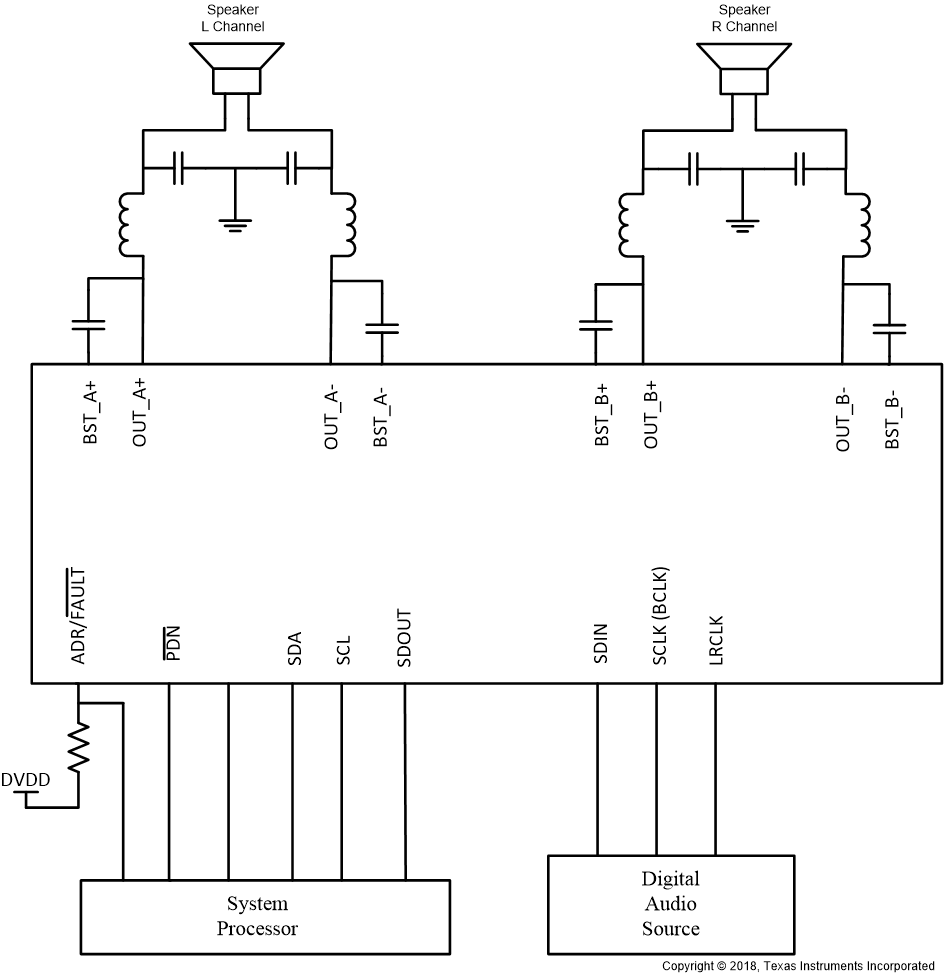
The TAS5805M is a high-efficiency, stereo, closed-loop Class-D amplifier offering a cost-effective digital-input solution with low power dissipation and sound enrichment. The device’s integrated audio processor and 96 kHz architecture support advanced audio process flow, including SRC, 15 BQs per channel, volume control, audio mixing, 3-band 4th order DRC, full-band AGL, THD manager and level meter.

Featuring TI's proprietary Hybrid Modulation scheme, the TAS5805M consumes very-low quiescent current (16.5 mA at 13.5 V PVDD), extending battery life in portable audio applications. With advanced EMI suppression technology, designers can leverage inexpensive ferrite bead filters to reduce board space and system cost.

Device Information
PART NUMBERPACKAGE(1)BODY SIZE (NOM)
TAS5805MTSSOP (28) PWP9.7 mm × 4.4 mm
For all available packages, see the orderable addendum at the end of the data sheet.
GUID-F64B14EC-8047-4F8F-A330-C7B1A2B49DE1-low.gifSimplified Block Diagram