SLOSEA8 December 2024 TAS5815
PRODUCTION DATA
- 1
- 1 Features
- 2 Applications
- 3 Description
- Device Comparison Table
- 4 Pin Configuration and Functions
- 5 Specifications
- 6 Typical Characteristics
-
7 Detailed Description
- 7.1 Overview
- 7.2 Functional Block Diagram
- 7.3 Feature Description
- 7.4 Device Functional Modes
- 7.5 Programming and Control
- 8 Register Maps
- 9 Application Information Disclaimer
- 10Power Supply Recommendations
- 11Layout
- 12Device and Documentation Support
- 13Revision History
- 14Mechanical and Packaging Information
Package Options
Mechanical Data (Package|Pins)
- PWP|28
Thermal pad, mechanical data (Package|Pins)
- PWP|28
Orderable Information
4 Pin Configuration and Functions
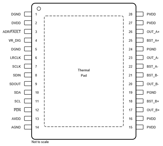
 Figure 4-1 PWP (TSSOP) Package, 28-Pin
PadDown, Top View
Figure 4-1 PWP (TSSOP) Package, 28-Pin
PadDown, Top ViewTable 4-1 Pin Functions For TSSOP28
Package
| PIN | TYPE(1) | DESCRIPTION | ||
|---|---|---|---|---|
| NO. | NAME | |||
| 1 | DGND | P | Digital ground | |
| 2 | DVDD | P | 3.3-V/1.8-V digital power supply | |
| 3 | ADR/FAULT | DI/O | A table of resistor value (Pull up/Down to DVDD/GND)
will decide device I2C address. After power up, this pin can be programmed by writing 1 to a register bit after Power up bit. In this mode, ADR/ FAULT is redefine as FAULT. |
|
| 4 | VR_DIG | P | Internally regulated 1.5-V digital supply voltage. This pin must not be used to drive external devices | |
| 5 | DGND | P | Digital ground | |
| 6 | LRCLK | DI | Input serial audio data left/right clock (sample rate clock) | |
| 7 | SCLK | DI | Serial audio data clock (shift clock). SCLK is the serial audio port input data bit clock. | |
| 8 | SDIN | DI | Serial audio data input. SDIN supports three discrete (stereo) data formats | |
| 9 | SDOUT | DO | Serail audio data output, the source data can select as Pre-DSP or Post-DSP. | |
| 10 | SDA | DI/O | I2C serial control data interface input/output | |
| 11 | SCL | DI | I2C serial control clock input | |
| 12 | PDN | DI | Power down, active-low. PDN sets the amplifier in Shutdown, turn off all internal regulators. | |
| 13 | AVDD | P | Internally regulated 5 V analog power voltage. This pin must not be used to drive external devices. | |
| 14 | AGND | G | Analog ground | |
| 15 | PVDD | P | PVDD voltage input | |
| 16 | PVDD | P | PVDD voltage input | |
| 17 | OUT_B+ | PO | Positive pin for differential speaker amplifier output B+ | |
| 18 | BST_B+ | P | Connection point for the OUT_B+ bootstrap capacitor which is used to create a power supply for the high-side gate drive for OUT_B+ | |
| 19 | PGND | G | Ground reference for power device circuitry. Connect this pin to system ground | |
| 20 | OUT_B- | NO | Negative pin for differential speaker amplifier output B- | |
| 21 | BST_B- | P | Connection point for the OUT_B- bootstrap capacitor which is used to create a power supply for the high-side gate drive for OUT_B- | |
| 22 | BST_A- | P | Connection point for the OUT_A- bootstrap capacitor which is used to create a power supply for the high-side gate drive for OUT_A- | |
| 23 | OUT_A- | NO | Negative pin for differential speaker amplifier output A- | |
| 24 | PGND | G | Ground reference for power device circuitry. Connect this pin to system ground | |
| 25 | BST_A+ | P | Connection point for the OUT_A+ bootstrap capacitor which is used to create a power supply for the high-side gate drive for OUT_A+ | |
| 26 | OUT_A+ | PO | Positive pin for differential speaker amplifier output A+ | |
| 27 | PVDD | P | PVDD voltage input | |
| 28 | PVDD | P | PVDD voltage input | |
| PowerPADTM | G | Ground, connect to grounded heat sink for best system performance. | ||
(1) AI = Analog input, AO = Analog
output, DI = Digital Input, DO = Digital Output, DI/O = Digital Bi-directional
(input and output), PO = Positive output, NO = Negative output, P = Power, G =
Ground (0 V)