SLOSEA8 December   2024 TAS5815

PRODUCTION DATA  

  1.   1
  2. Features
  3. Applications
  4. Description
  5.   Device Comparison Table
  6. Pin Configuration and Functions
  7. Specifications
    1. 5.1 Absolute Maximum Ratings
    2. 5.2 ESD Ratings
    3. 5.3 Recommended Operating Conditions
    4. 5.4 Thermal Information
    5. 5.5 Electrical Characteristics
    6. 5.6 Timing Requirements
  8. Typical Characteristics
    1. 6.1 Bridge Tied Load (BTL) Configuration Curves with BD Modulation
    2. 6.2 Bridge Tied Load (BTL) Configuration Curves with 1SPW Modulation
    3. 6.3 Parallel Bridge Tied Load (PBTL) Configuration With BD Modulation
    4. 6.4 Parallel Bridge Tied Load (PBTL) Configuration With 1SPW Modulation
  9. Detailed Description
    1. 7.1 Overview
    2. 7.2 Functional Block Diagram
    3. 7.3 Feature Description
      1. 7.3.1 Power Supplies
      2. 7.3.2 Device Clocking
      3. 7.3.3 Serial Audio Port – Clock Rates
      4. 7.3.4 Serial Audio Port - Data Formats and Bit Depths
      5. 7.3.5 Clock Halt Auto-recovery
      6. 7.3.6 Sample Rate on the Fly Change
      7. 7.3.7 Digital Audio Processing
      8. 7.3.8 Class D Audio Amplifier
        1. 7.3.8.1 Speaker Amplifier Gain Select
    4. 7.4 Device Functional Modes
      1. 7.4.1 Software Control
      2. 7.4.2 Speaker Amplifier Operating Modes
        1. 7.4.2.1 BTL Mode
        2. 7.4.2.2 PBTL Mode
      3. 7.4.3 Low EMI Modes
        1. 7.4.3.1 Minimize EMI with Spread Spectrum
        2. 7.4.3.2 Minimize EMI with channel to channel phase shift
        3. 7.4.3.3 Minimize EMI with Multi-Devices PWM Phase Synchronization
      4. 7.4.4 Thermal Foldback
      5. 7.4.5 Device State Control
      6. 7.4.6 Device Modulation
        1. 7.4.6.1 BD Modulation
        2. 7.4.6.2 1SPW Modulation
        3. 7.4.6.3 Hybrid Modulation
      7. 7.4.7 Load Detect
        1. 7.4.7.1 Short Load Detect
        2. 7.4.7.2 Open Load Detect
    5. 7.5 Programming and Control
      1. 7.5.1 I2C Serial Communication Bus
      2. 7.5.2 Target Address
        1. 7.5.2.1 Random Write
        2. 7.5.2.2 Random Read
        3. 7.5.2.3 Sequential Write
        4. 7.5.2.4 Sequential Read
        5. 7.5.2.5 DSP Memory Book, Page and BQ update
        6. 7.5.2.6 Example Use
        7. 7.5.2.7 Checksum
          1. 7.5.2.7.1 Cyclic Redundancy Check (CRC) Checksum
          2. 7.5.2.7.2 Exclusive or (XOR) Checksum
      3. 7.5.3 Control via Software
        1. 7.5.3.1 Startup Procedures
        2. 7.5.3.2 Shutdown Procedures
        3. 7.5.3.3 Protection and Monitoring
          1. 7.5.3.3.1 Overcurrent Shutdown (OCSD)
          2. 7.5.3.3.2 DC Detect
          3. 7.5.3.3.3 Device Over Temperature Protection
          4. 7.5.3.3.4 Over Voltage Protection
          5. 7.5.3.3.5 Under Voltage Protection
          6. 7.5.3.3.6 Clock Fault
  10. Register Maps
    1. 8.1 CONTROL PORT Registers
  11. Application Information Disclaimer
    1. 9.1 Application Information
      1. 9.1.1 Bootstrap Capacitors
      2. 9.1.2 Inductor Selections
      3. 9.1.3 Power Supply Decoupling
      4. 9.1.4 Output EMI Filtering
    2. 9.2 Typical Application
      1. 9.2.1 2.0 (Stereo BTL) System
        1. 9.2.1.1 Design Requirements
      2. 9.2.2 Detailed Design Procedure
        1. 9.2.2.1 Step 1: Hardware Integration
        2. 9.2.2.2 Step 2: Speaker Tuning
        3. 9.2.2.3 Step 3: Software Integration
      3. 9.2.3 MONO (PBTL) System
        1. 9.2.3.1 Design Requirements
      4. 9.2.4 Advanced 2.1 System (Two TAS5815 Devices)
  12. 10Power Supply Recommendations
    1. 10.1 DVDD Supply
    2. 10.2 PVDD Supply
  13. 11Layout
    1. 11.1 Layout Guidelines
      1. 11.1.1 General Guidelines for Audio Amplifiers
      2. 11.1.2 Importance of PVDD Bypass Capacitor Placement on PVDD Network
      3. 11.1.3 Optimizing Thermal Performance
        1. 11.1.3.1 Device, Copper, and Component Layout
        2. 11.1.3.2 Stencil Pattern
          1. 11.1.3.2.1 PCB footprint and Via Arrangement
          2. 11.1.3.2.2 Solder Stencil
    2. 11.2 Layout Example
  14. 12Device and Documentation Support
    1. 12.1 Device Support
      1. 12.1.1 Device Nomenclature
    2. 12.2 Support Resources
    3. 12.3 Trademarks
    4. 12.4 Electrostatic Discharge Caution
    5. 12.5 Glossary
  15. 13Revision History
  16. 14Mechanical and Packaging Information
    1. 14.1 Package Option Addendum

Package Options

Mechanical Data (Package|Pins)
Thermal pad, mechanical data (Package|Pins)
Orderable Information

Serial Audio Port - Data Formats and Bit Depths

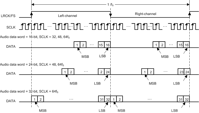
The serial audio interface port is a 3-wire serial port with the signals LRCK/FS, SCK, and SDIN. SCK is the serial audio bit clock, used to clock the serial data present on SDIN into the serial shift register of the audio interface. Serial data is clocked into the device on the rising edge of SCK. The LRCK/FS pin is the serial audio left/right word clock or frame sync when the device is operated in TDM Mode.

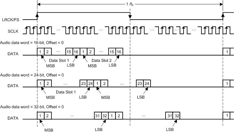
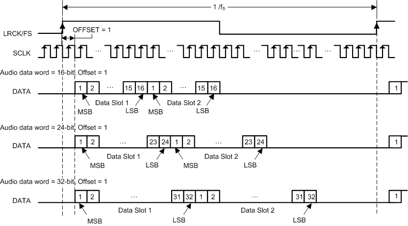
TAS5815 supports industry-standard audio data formats, including standard I2S, left-justified, right-justified and TDM/DSP data. Data formats are selected via Register (Page0-Register 0x33 [5:4]). If the high width of LRCK/FS in TDM/DSP mode is less than 8 cycles of SCK, the register (Page0-Register 0x33 [3:2]) should set to 01. All formats require binary two's complement, MSB-first audio data; up to 32-bit audio data is accepted. All the data formats, word length and clock rate supported by this device are shown in Table 7-1. The data formats are detailed in Figure 6-1 through Figure 6-110. The word length are selected via Register (Page0-Register 0x33 [1:0]). The offsets of data are selected via Register (Page0-Register 0x33 [7]) and Register (Page0-Register 0x34 [7:0]). Default setting is I2S and 24 bit word length.
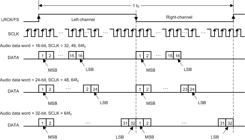
TAS5815 Left Justified Audio Data FormatFigure 7-2 Left Justified Audio Data Format
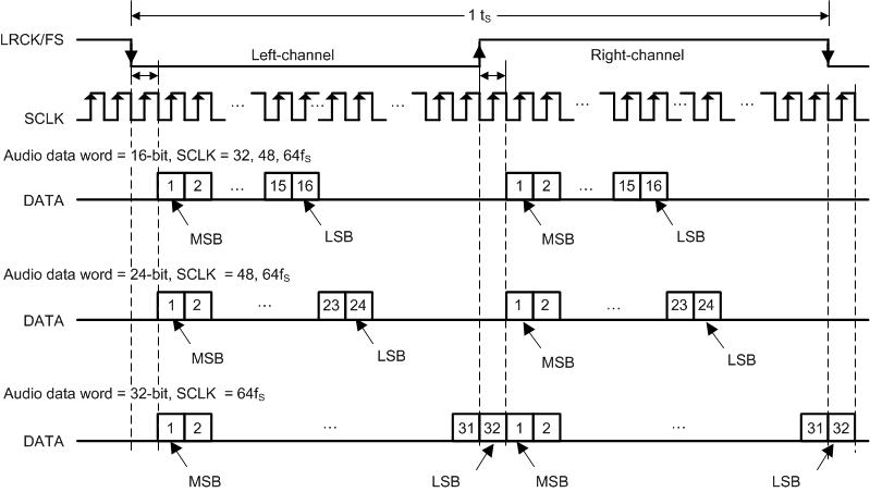
TAS5815 I2S Audio Data Format
I2S Data Format; L-channel = LOW, R-channel = HIGH
Figure 7-3 I2S Audio Data Format
TAS5815 Right Justified Audio Data Format
Right Justified Data Format; L-channel = HIGH, R-channel = LOW
Figure 7-4 Right Justified Audio Data Format
TAS5815 TDM 1 Audio Data Format
TDM Data Format with OFFSET = 0
In TDM Modes, Duty Cycle of LRCK/FS should be 1x SCLK at minimum. Rising edge is considered frame start.
Figure 7-5 TDM 1 Audio Data Format
TAS5815 TDM 2 Audio Data Format
TDM Data Format with OFFSET = 1
In TDM Modes, Duty Cycle of LRCK/FS should be 1x SCLK at minimum. Rising edge is considered frame start.
Figure 7-6 TDM 2 Audio Data Format