SLOSE66 november 2020 TAS6424MS-Q1
PRODUCTION DATA
- 1 Features
- 2 Applications
- 3 Description
- 4 Revision History
- 5 Device Options
- 6 Pin Configuration and Functions
- 7 Specifications
- 8 Parameter Measurement Information
-
9 Detailed Description
- 9.1 Overview
- 9.2 Functional Block Diagram
- 9.3
Feature Description
- 9.3.1 Serial Audio Port
- 9.3.2 High-Pass Filter
- 9.3.3 Volume Control and Gain
- 9.3.4 High-Frequency Pulse-Width Modulator (PWM)
- 9.3.5 Channel-to-Channel Phase Control
- 9.3.6 Gate Drive
- 9.3.7 Power FETs
- 9.3.8 Load Diagnostics
- 9.3.9
Protection and Monitoring
- 9.3.9.1 Overcurrent Limit (ILIMIT)
- 9.3.9.2 Overcurrent Shutdown (ISD)
- 9.3.9.3 DC Detect
- 9.3.9.4 Clip Detect
- 9.3.9.5 Global Overtemperature Warning (OTW), Overtemperature Shutdown (OTSD)
- 9.3.9.6 Channel Overtemperature Warning [OTW(i)] and Shutdown [OTSD(i)]
- 9.3.9.7 Undervoltage (UV) and Power-On-Reset (POR)
- 9.3.9.8 Overvoltage (OV) and Load Dump
- 9.3.10 Power Supply
- 9.3.11 Hardware Control Pins
- 9.4 Device Functional Modes
- 9.5 Programming
- 9.6
Register Maps
- 9.6.1 Mode Control Register (address = 0x00) [default = 0x00]
- 9.6.2 Miscellaneous Control 1 Register (address = 0x01) [default = 0x32]
- 9.6.3 Miscellaneous Control 2 Register (address = 0x02) [default = 0x62]
- 9.6.4 SAP Control (Serial Audio-Port Control) Register (address = 0x03) [default = 0x04]
- 9.6.5 Channel State Control Register (address = 0x04) [default = 0x55]
- 9.6.6 Channel 1 Through 4 Volume Control Registers (address = 0x05–0x08) [default = 0xCF]
- 9.6.7 DC Load Diagnostic Control 1 Register (address = 0x09) [default = 0x00]
- 9.6.8 DC Load Diagnostic Control 2 Register (address = 0x0A) [default = 0x11]
- 9.6.9 DC Load Diagnostic Control 3 Register (address = 0x0B) [default = 0x11]
- 9.6.10 DC Load Diagnostic Report 1 Register (address = 0x0C) [default = 0x00]
- 9.6.11 DC Load Diagnostic Report 2 Register (address = 0x0D) [default = 0x00]
- 9.6.12 DC Load Diagnostics Report 3 Line Output Register (address = 0x0E) [default = 0x00]
- 9.6.13 Channel State Reporting Register (address = 0x0F) [default = 0x55]
- 9.6.14 Channel Faults (Overcurrent, DC Detection) Register (address = 0x10) [default = 0x00]
- 9.6.15 Global Faults 1 Register (address = 0x11) [default = 0x00]
- 9.6.16 Global Faults 2 Register (address = 0x12) [default = 0x00]
- 9.6.17 Warnings Register (address = 0x13) [default = 0x20]
- 9.6.18 Pin Control Register (address = 0x14) [default = 0x00]
- 9.6.19 AC Load Diagnostic Control 1 Register (address = 0x15) [default = 0x00]
- 9.6.20 AC Load Diagnostic Control 2 Register (address = 0x16) [default = 0x00]
- 9.6.21 AC Load Diagnostic Impedance Report Ch1 through Ch4 Registers (address = 0x17–0x1A) [default = 0x00]
- 9.6.22 AC Load Diagnostic Phase Report High Register (address = 0x1B) [default = 0x00]
- 9.6.23 AC Load Diagnostic Phase Report Low Register (address = 0x1C) [default = 0x00]
- 9.6.24 AC Load Diagnostic STI Report High Register (address = 0x1D) [default = 0x00]
- 9.6.25 AC Load Diagnostic STI Report Low Register (address = 0x1E) [default = 0x00]
- 9.6.26 Miscellaneous Control 3 Register (address = 0x21) [default = 0x00]
- 9.6.27 Clip Control Register (address = 0x22) [default = 0x01]
- 9.6.28 Clip Window Register (address = 0x23) [default = 0x14]
- 9.6.29 Clip Warning Register (address = 0x24) [default = 0x00]
- 9.6.30 ILIMIT Status Register (address = 0x25) [default = 0x00]
- 9.6.31 Miscellaneous Control 4 Register (address = 0x26) [default = 0x40]
- 10Application Information Disclaimer
- 11Power Supply Recommendations
- 12Layout
- 13Device and Documentation Support
- 14Mechanical, Packaging, and Orderable Information
Package Options
Mechanical Data (Package|Pins)
- DKQ|56
Thermal pad, mechanical data (Package|Pins)
- DKQ|56
Orderable Information
3 Description
The TAS6424MS-Q1 device is a four-channel digital-input Class-D audio amplifier that implements a 2.1 MHz PWM switching frequency enabling a cost-optimized solution in a very small PCB size, full operation down to 4.5 V for start/stop events, and exceptional sound quality with up to 40 kHz audio bandwidth.
The output switching frequency can be set either above the AM band, which eliminates AM-band interferences and reduces output filtering and cost, or below the AM band to optimize efficiency.
The device has a built-in load diagnostic function for detecting and diagnosing misconnected outputs as well as detection of AC-coupled tweeters to help to reduce test time during the manufacturing process.
The TAS6424MS-Q1 Class-D audio amplifier is designed for use in automotive head units and external amplifier modules. For pin compatible one, two and four-channel devices see the the Device Options table.
| PART NUMBER | PACKAGE(1) | BODY SIZE (NOM) |
|---|---|---|
| TAS6424MS-Q1 | HSSOP (56) | 18.41 mm × 7.49 mm |
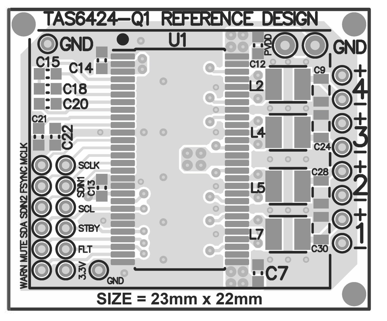
 PCB AREA