SLOSE66 november 2020 TAS6424MS-Q1
PRODUCTION DATA
- 1 Features
- 2 Applications
- 3 Description
- 4 Revision History
- 5 Device Options
- 6 Pin Configuration and Functions
- 7 Specifications
- 8 Parameter Measurement Information
-
9 Detailed Description
- 9.1 Overview
- 9.2 Functional Block Diagram
- 9.3
Feature Description
- 9.3.1 Serial Audio Port
- 9.3.2 High-Pass Filter
- 9.3.3 Volume Control and Gain
- 9.3.4 High-Frequency Pulse-Width Modulator (PWM)
- 9.3.5 Channel-to-Channel Phase Control
- 9.3.6 Gate Drive
- 9.3.7 Power FETs
- 9.3.8 Load Diagnostics
- 9.3.9
Protection and Monitoring
- 9.3.9.1 Overcurrent Limit (ILIMIT)
- 9.3.9.2 Overcurrent Shutdown (ISD)
- 9.3.9.3 DC Detect
- 9.3.9.4 Clip Detect
- 9.3.9.5 Global Overtemperature Warning (OTW), Overtemperature Shutdown (OTSD)
- 9.3.9.6 Channel Overtemperature Warning [OTW(i)] and Shutdown [OTSD(i)]
- 9.3.9.7 Undervoltage (UV) and Power-On-Reset (POR)
- 9.3.9.8 Overvoltage (OV) and Load Dump
- 9.3.10 Power Supply
- 9.3.11 Hardware Control Pins
- 9.4 Device Functional Modes
- 9.5 Programming
- 9.6
Register Maps
- 9.6.1 Mode Control Register (address = 0x00) [default = 0x00]
- 9.6.2 Miscellaneous Control 1 Register (address = 0x01) [default = 0x32]
- 9.6.3 Miscellaneous Control 2 Register (address = 0x02) [default = 0x62]
- 9.6.4 SAP Control (Serial Audio-Port Control) Register (address = 0x03) [default = 0x04]
- 9.6.5 Channel State Control Register (address = 0x04) [default = 0x55]
- 9.6.6 Channel 1 Through 4 Volume Control Registers (address = 0x05–0x08) [default = 0xCF]
- 9.6.7 DC Load Diagnostic Control 1 Register (address = 0x09) [default = 0x00]
- 9.6.8 DC Load Diagnostic Control 2 Register (address = 0x0A) [default = 0x11]
- 9.6.9 DC Load Diagnostic Control 3 Register (address = 0x0B) [default = 0x11]
- 9.6.10 DC Load Diagnostic Report 1 Register (address = 0x0C) [default = 0x00]
- 9.6.11 DC Load Diagnostic Report 2 Register (address = 0x0D) [default = 0x00]
- 9.6.12 DC Load Diagnostics Report 3 Line Output Register (address = 0x0E) [default = 0x00]
- 9.6.13 Channel State Reporting Register (address = 0x0F) [default = 0x55]
- 9.6.14 Channel Faults (Overcurrent, DC Detection) Register (address = 0x10) [default = 0x00]
- 9.6.15 Global Faults 1 Register (address = 0x11) [default = 0x00]
- 9.6.16 Global Faults 2 Register (address = 0x12) [default = 0x00]
- 9.6.17 Warnings Register (address = 0x13) [default = 0x20]
- 9.6.18 Pin Control Register (address = 0x14) [default = 0x00]
- 9.6.19 AC Load Diagnostic Control 1 Register (address = 0x15) [default = 0x00]
- 9.6.20 AC Load Diagnostic Control 2 Register (address = 0x16) [default = 0x00]
- 9.6.21 AC Load Diagnostic Impedance Report Ch1 through Ch4 Registers (address = 0x17–0x1A) [default = 0x00]
- 9.6.22 AC Load Diagnostic Phase Report High Register (address = 0x1B) [default = 0x00]
- 9.6.23 AC Load Diagnostic Phase Report Low Register (address = 0x1C) [default = 0x00]
- 9.6.24 AC Load Diagnostic STI Report High Register (address = 0x1D) [default = 0x00]
- 9.6.25 AC Load Diagnostic STI Report Low Register (address = 0x1E) [default = 0x00]
- 9.6.26 Miscellaneous Control 3 Register (address = 0x21) [default = 0x00]
- 9.6.27 Clip Control Register (address = 0x22) [default = 0x01]
- 9.6.28 Clip Window Register (address = 0x23) [default = 0x14]
- 9.6.29 Clip Warning Register (address = 0x24) [default = 0x00]
- 9.6.30 ILIMIT Status Register (address = 0x25) [default = 0x00]
- 9.6.31 Miscellaneous Control 4 Register (address = 0x26) [default = 0x40]
- 10Application Information Disclaimer
- 11Power Supply Recommendations
- 12Layout
- 13Device and Documentation Support
- 14Mechanical, Packaging, and Orderable Information
Package Options
Mechanical Data (Package|Pins)
- DKQ|56
Thermal pad, mechanical data (Package|Pins)
- DKQ|56
Orderable Information
10.1.4 Line Driver Applications
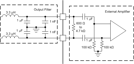
In many automotive audio applications, the same head unit must drive either a speaker (with several ohms of impedance) or an external amplifier input (with several kΩ of impedance). The design is capable of supporting both applications and has special line-drive gain and diagnostics. Coupled with the high switching frequency, the device is well suited for this type of application. Set the desired channel in line driver mode through I2C register 0x00, the externally connected amplifier must have a differential impedance from 600 Ω to 4.7 kΩ for the DC line diagnostic to detect the connected external amplifier. Figure 10-1 shows the recommended external amplifier input configuration.
 Figure 10-1 External Amplifier Input Configuration for Line Driver