SLOSE88 December   2024 TAS6754-Q1

ADVANCE INFORMATION  

  1.   1
  2. Features
  3. Applications
  4. Description
  5. Pin Configuration and Functions
  6. Specifications
    1. 5.1 Absolute Maximum Ratings
    2. 5.2 Recommended Operating Conditions
    3. 5.3 ESD Ratings
    4. 5.4 Thermal Information
    5. 5.5 Electrical Characteristics
    6. 5.6 Typical Characteristics
  7. Parameter Measurement Information
  8. Detailed Description
    1. 7.1 Overview
    2. 7.2 Functional Block Diagram
    3. 7.3 Feature Description
      1. 7.3.1 Power Supply
        1. 7.3.1.1 Power-Supply Sequence
          1. 7.3.1.1.1 Power-Up Sequence
          2. 7.3.1.1.2 Power-Down Sequence
        2. 7.3.1.2 Device Initialization and Power-On-Reset (POR)
      2. 7.3.2 Serial Audio Port
        1. 7.3.2.1 Left-Justified Timing
        2. 7.3.2.2 I2S Mode
        3. 7.3.2.3 DSP Mode
        4. 7.3.2.4 TDM Mode
        5. 7.3.2.5 SDOUT - Data Output
        6. 7.3.2.6 Device Clocking
          1. 7.3.2.6.1 Clock Rates
          2. 7.3.2.6.2 Clock Halt Auto-recovery
          3. 7.3.2.6.3 Sample Rate on the Fly Change
        7. 7.3.2.7 Clock Error Handling
      3. 7.3.3 Digital Audio Processing
        1. 7.3.3.1 PVDD Foldback
        2. 7.3.3.2 High-Pass Filter
        3. 7.3.3.3 Analog Gain
        4. 7.3.3.4 Digital Volume Control
          1. 7.3.3.4.1 Auto Mute
        5. 7.3.3.5 Gain Compensation Biquads
        6. 7.3.3.6 Low Latency Signal Path
        7. 7.3.3.7 Full Feature Low Latency Path
      4. 7.3.4 Class-D operation and Spread Spectrum Control
        1. 7.3.4.1 1L Modulation
        2. 7.3.4.2 High-Frequency Pulse-Width Modulator (PWM)
        3. 7.3.4.3 Spread Spectrum Control
        4. 7.3.4.4 Gate Drive
        5. 7.3.4.5 Power FETs
      5. 7.3.5 Load Diagnostics
        1. 7.3.5.1 DC Load Diagnostics
          1. 7.3.5.1.1 Automatic DC Load Diagnostics at Device Initialization
          2. 7.3.5.1.2 Automatic DC load diagnostics during Hi-Z or PLAY
          3. 7.3.5.1.3 Manual start of DC load diagnostics
          4. 7.3.5.1.4 Short-to-Ground
          5. 7.3.5.1.5 Short-to-Power
          6. 7.3.5.1.6 Shorted-Load and Open-Load
        2. 7.3.5.2 Line Output Diagnostics
        3. 7.3.5.3 AC Load Diagnostics
          1. 7.3.5.3.1 Operating Principal
          2. 7.3.5.3.2 Stimulus
          3. 7.3.5.3.3 Load Impedance
          4. 7.3.5.3.4 Tweeter Detection
        4. 7.3.5.4 Real-Time Load Diagnostics
        5. 7.3.5.5 DC Resistance Measurement
      6. 7.3.6 Protection and Monitoring
        1. 7.3.6.1 Overcurrent Limit (Cycle-By-Cycle)
        2. 7.3.6.2 Overcurrent Shutdown
        3. 7.3.6.3 Current Sense
        4. 7.3.6.4 DC Detect
        5. 7.3.6.5 Digital Clip Detect
        6. 7.3.6.6 Charge Pump
        7. 7.3.6.7 Temperature Protection and Monitoring
          1. 7.3.6.7.1 Overtemperature Shutdown
          2. 7.3.6.7.2 Overtemperature Warning
          3. 7.3.6.7.3 Thermal Gain Foldback
        8. 7.3.6.8 Power Failures
      7. 7.3.7 Hardware Control Pins
        1. 7.3.7.1 FAULT Pin
        2. 7.3.7.2 PD Pin
        3. 7.3.7.3 STBY Pin
        4. 7.3.7.4 GPIO Pins
          1. 7.3.7.4.1 General Purpose Input
          2. 7.3.7.4.2 General Purpose Output
        5. 7.3.7.5 Advanced GPIO functions
          1. 7.3.7.5.1 Clock Synchronization
            1. 7.3.7.5.1.1 External SYNC signal (GPIO sync)
            2. 7.3.7.5.1.2 Synchronization through the audio serial clock (SCLK)
            3. 7.3.7.5.1.3 TAS6754-Q1 as clock source for external devices
    4. 7.4 Device Functional Modes
      1. 7.4.1 Internal Reporting Signals
        1. 7.4.1.1 Fault Signal
        2. 7.4.1.2 Warning Signal
      2. 7.4.2 Device States and Flags
        1. 7.4.2.1 Audio Channel States
          1. 7.4.2.1.1 SHUTDOWN State
          2. 7.4.2.1.2 DEEP SLEEP State
          3. 7.4.2.1.3 LOAD DIAG State
          4. 7.4.2.1.4 SLEEP State
          5. 7.4.2.1.5 Hi-Z State
          6. 7.4.2.1.6 PLAY State
          7. 7.4.2.1.7 FAULT State
          8. 7.4.2.1.8 Auto Recovery (AUTOREC) State
        2. 7.4.2.2 Status and Memory Registers
      3. 7.4.3 Fault Events
        1. 7.4.3.1 Power Fault Events
          1. 7.4.3.1.1 DVDD Power-On-Reset (POR)
          2. 7.4.3.1.2 DVDD Undervoltage Fault
          3. 7.4.3.1.3 VBAT Undervoltage Fault
          4. 7.4.3.1.4 PVDD Overvoltage Fault
          5. 7.4.3.1.5 PVDD Undervoltage Fault
        2. 7.4.3.2 Overtemperature Shutdown (OTSD) Event
        3. 7.4.3.3 Overcurrent Limit Fault Event
        4. 7.4.3.4 Overcurrent Shutdown Event
        5. 7.4.3.5 DC Fault Event
        6. 7.4.3.6 Clock Error Event
        7. 7.4.3.7 Charge Pump Fault Event
      4. 7.4.4 Warning Events
        1. 7.4.4.1 Overtemperature Warning Event
        2. 7.4.4.2 Overcurrent Limit Warning Event
        3. 7.4.4.3 Clip Detect Warning Event
    5. 7.5 Programming
      1. 7.5.1 I2C Serial Communication Bus
      2. 7.5.2 I2C Address Selection
      3. 7.5.3 I2C Bus Protocol
      4. 7.5.4 Random Write
      5. 7.5.5 Sequential Write
      6. 7.5.6 Random Read
      7. 7.5.7 Sequential Read
  9. Application Information Disclaimer
    1. 8.1 Application Information
      1. 8.1.1 Reconstruction Filter Design
    2. 8.2 Typical Application
      1. 8.2.1 BTL Application
    3. 8.3 Power Supply Recommendations
    4. 8.4 Layout
      1. 8.4.1 Layout Guidelines
        1. 8.4.1.1 Electrical Connection of Thermal pad and Heat Sink
        2. 8.4.1.2 EMI Considerations
        3. 8.4.1.3 General Guidelines
      2. 8.4.2 Layout Example
      3. 8.4.3 Thermal Considerations
  10. Device and Documentation Support
    1. 9.1 Documentation Support
      1. 9.1.1 Related Documentation
    2. 9.2 Receiving Notification of Documentation Updates
    3. 9.3 Support Resources
    4. 9.4 Trademarks
    5. 9.5 Electrostatic Discharge Caution
    6. 9.6 Glossary
  11. 10Revision History
  12. 11Mechanical, Packaging, and Orderable Information

Package Options

Mechanical Data (Package|Pins)
Thermal pad, mechanical data (Package|Pins)
Orderable Information
Thermal Gain Foldback

Thermal Gain Foldback (TGFB) is a power limiting feature to protect the TAS6754-Q1 from excessive die temperature while maintaining audio output.

The main purpose of foldback power limiting is to keep the output stage within its safe power dissipation limit to avoid unexpected Overtemperature Shutdown. The feature provides a smooth audio response and allows for uninterrupted music playback when temperature limits are crossed. That means the TAS6754-Q1 does not simply shut down, but continues to operate with considerable music output power while avoiding the trigger of OTSD.

The DSP of TAS6754-Q1 monitors the die temperature continuously in real-time for safe operation. The device can warn the host if the die temperature is approaching the OTW limits. TAS6754-Q1 still functions until the temperature reaches the OTSD threshold, at which either individual channels or the amplifier is shut down.

If the channel die temperature rises above the configured foldback level, the thermal gain foldback circuit initially activates. The device starts to reduce the gain in steps of 0.25dB per sample and thereby output power. This attack rate can be configured. The configured max attenuations are individual to the level and do not stack between levels.

When the temperature decreases below the foldback level, the attenuation will be held for a configurable number of samples before the attenuation will begin releasing at the gain step rate of 0.1dB per sample. This release rate of the TGFB can be programmed.
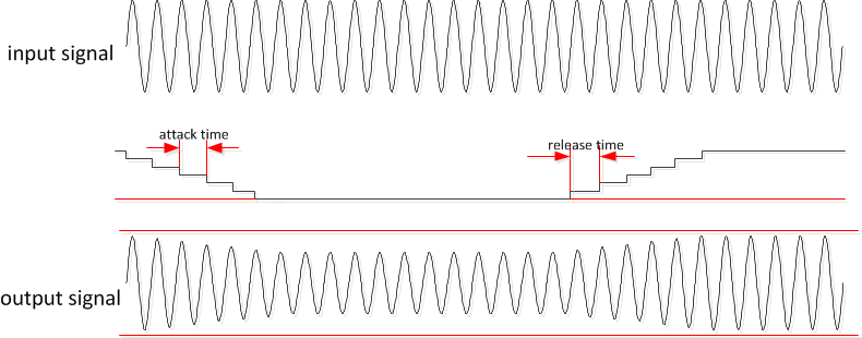
TAS6754-Q1 Thermal Foldback Attack and ReleaseFigure 7-18 Thermal Foldback Attack and Release