SCPS222C May 2010 – October 2015 TCA8418E
PRODUCTION DATA.
- 1 Features
- 2 Applications
- 3 Description
- 4 Revision History
- 5 Pin Configuration and Functions
-
6 Specifications
- 6.1 Absolute Maximum Ratings
- 6.2 ESD Ratings
- 6.3 Recommended Operating Conditions
- 6.4 Thermal Information
- 6.5 Electrical Characteristics
- 6.6 I2C Interface Timing Requirements
- 6.7 Reset Timing Requirements for Standard Mode, Fast Mode, Fast Mode Plus (FM+) I2C Bus
- 6.8 Switching Characteristics for Standard Mode, Fast Mode, Fast Mode Plus (FM+) I2C Bus
- 6.9 Keypad Switching Characteristics for Standard Mode, Fast Mode, Fast Mode Plus (FM+) I2C Bus
- 6.10 Typical Characteristics
- 7 Parameter Measurement Information
-
8 Detailed Description
- 8.1 Overview
- 8.2 Functional Block Diagram
- 8.3 Feature Description
- 8.4 Device Functional Modes
- 8.5 Programming
- 8.6
Register Maps
- 8.6.1 Device Address
- 8.6.2
Control Register and Command Byte
- 8.6.2.1 Configuration Register (Address 0x01)
- 8.6.2.2 Interrupt Status Register, INT_STAT (Address 0x02)
- 8.6.2.3 Key Lock and Event Counter Register, KEY_LCK_EC (Address 0x03)
- 8.6.2.4 Key Event Registers (FIFO), KEY_EVENT_A-J (Address 0x04-0x0D)
- 8.6.2.5 Keypad Lock1 to Lock2 Timer Register, KP_LCK_TIMER (Address 0x0E)
- 8.6.2.6 Unlock1 and Unlock2 Registers, UNLOCK1/2 (Address 0x0F-0x10)
- 8.6.2.7 GPIO Interrupt Status Registers, GPIO_INT_STAT1-3 (Address 0x11-0x13)
- 8.6.2.8 GPIO Data Status Registers, GPIO_DAT_STAT1-3 (Address 0x14-0x16)
- 8.6.2.9 GPIO Data Out Registers, GPIO_DAT_OUT1-3 (Address 0x17-0x19)
- 8.6.2.10 GPIO Interrupt Enable Registers, GPIO_INT_EN1-3 (Address 0x1A-0x1C)
- 8.6.2.11 Keypad or GPIO Selection Registers, KP_GPIO1-3 (Address 0x1D-0x1F)
- 8.6.2.12 GPI Event Mode Registers, GPI_EM1-3 (Address 0x20-0x22)
- 8.6.2.13 GPIO Data Direction Registers, GPIO_DIR1-3 (Address 0x23-0x25)
- 8.6.2.14 GPIO Edge/Level Detect Registers, GPIO_INT_LVL1-3 (Address 0x26-0x28)
- 8.6.2.15 Debounce Disable Registers, DEBOUNCE_DIS1-3 (Address 0x29-0x2B)
- 8.6.2.16 GPIO Pullup Disable Register, GPIO_PULL1-3 (Address 0x2C-0x2E)
- 9 Application and Implementation
- 10Power Supply Recommendations
- 11Layout
- 12Device and Documentation Support
- 13Mechanical, Packaging, and Orderable Information
Package Options
Mechanical Data (Package|Pins)
- YFP|25
Thermal pad, mechanical data (Package|Pins)
Orderable Information
1 Features
- Operating Power-Supply Voltage Range of 1.65-V to 3.6-V
- ±15-kV Human Body Model High Voltage ESD (GPIO lines)
- Supports 80 Buttons With Use of 18 GPIOs
- Supports QWERTY Keypad Operation Plus GPIO Expansion
- Low Standby (Idle) Current Consumption: 3 μA
- Supports 1-MHz Fast Mode Plus I2C Bus
- 10-Byte FIFO to Store 10 Key Presses and Releases
- Open-Drain Active-Low Interrupt Output
- Integrated Debounce Time of 50 μs
- Schmitt-Trigger Action Allows Slow Input Transition and Better Switching Noise Immunity at the SCL and SDA Inputs: Typical Vhys at 1.8 V is 0.18 V
- Latch-Up Performance Exceeds 200 mA Per JESD 78, Class II
- Very Small Package
- WCSP (YFP): 2 mm × 2 mm; 0.4 mm pitch
2 Applications
- Smart Phones
- Tablets
- HMI Panels
- GPS Devices
- MP3 Players
- Digital Cameras
3 Description
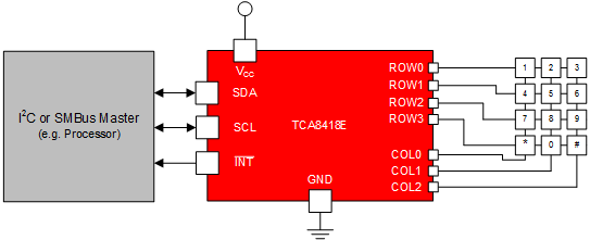
The TCA8418E is a keypad scan device with integrated ESD protection. It can operate from 1.65 V to 3.6 V and has 18 general purpose inputs/outputs (GPIO) that can be used to support up to 80 keys via the I2C interface.
The TCA8418E saves power and bandwidths since it handles the keypad scanning algorithms. The TCA8418E is also ideal for usage with processors that have limited GPIOs.
The key controller debounces inputs and maintains a 10 byte FIFO of key-press and release events which can store up to 10 keys with overflow wrap capability. An interrupt (INT) output can be configured to alert key presses and releases either as they occur, or at maximum rate. A CAD_INT pin is included to indicate the detection of CTRL-ALT-DEL (essentially, 1, 11, 21) key press action.
Device Information(1)
| PART NUMBER | PACKAGE | BODY SIZE (NOM) |
|---|---|---|
| TCA8418E | DSBGA (25) | 2.00 mm × 2.00 mm |
- For all available packages, see the orderable addendum at the end of the data sheet.
Simplified Schematic
