SCPS225E August   2011  – October 2024 TCA9509

PRODUCTION DATA  

  1.   1
  2. Features
  3. Applications
  4. Description
  5. Pin Configuration and Functions
  6. Specifications
    1. 5.1 Absolute Maximum Ratings
    2. 5.2 ESD Ratings
    3. 5.3 Recommended Operating Conditions
    4. 5.4 Thermal Information
    5. 5.5 Electrical Characteristics
    6. 5.6 Timing Requirements
    7. 5.7 I2C Interface Timing Requirements
  7. Parameter Measurement Information
  8. Detailed Description
    1. 7.1 Overview
    2. 7.2 Functional Block Diagram
    3. 7.3 Feature Description
      1. 7.3.1 Two-Channel Bidirectional Buffer
      2. 7.3.2 Integrated A-Side Current Source
      3. 7.3.3 Standard Mode and Fast Mode Support
    4. 7.4 Device Functional Modes
  9. Application and Implementation
    1. 8.1 Application Information
    2. 8.2 Typical Application
      1. 8.2.1 Design Requirements
      2. 8.2.2 Detailed Design Procedure
        1. 8.2.2.1 Clock Stretching Support
        2. 8.2.2.2 VILC and Pulldown Strength Requirements
  10. Power Supply Recommendations
  11. 10Layout
    1. 10.1 Layout Guidelines
    2. 10.2 Layout Example
  12. 11Device and Documentation Support
    1. 11.1 Receiving Notification of Documentation Updates
    2. 11.2 Support Resources
    3. 11.3 Trademarks
    4. 11.4 Electrostatic Discharge Caution
    5. 11.5 Glossary
  13. 12Revision History
  14. 13Mechanical, Packaging, and Orderable Information
    1. 13.1 Tape and Reel Information

Package Options

Mechanical Data (Package|Pins)
Thermal pad, mechanical data (Package|Pins)
Orderable Information

Applications

  • Servers
  • Routers (Telecom Switching Equipment)
  • Industrial Equipment
  • Products with many I2C targets and or long PCB Traces
Device Information
PART NUMBER PACKAGE (1) BODY SIZE (NOM)
TCA9509 VSSOP (8) 3.00mm × 3.00mm
X2QFN (8) 1.60mm × 1.60mm
For all available packages, see the orderable addendum at the end of the data sheet.
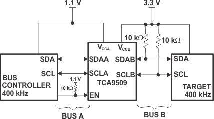
TCA9509 Simplified Schematic Simplified Schematic