SCPS254D January   2014  – October 2021 TCA9539-Q1

PRODUCTION DATA  

  1. Features
  2. Applications
  3. Description
  4. Revision History
  5. Pin Configuration and Functions
  6. Specifications
    1. 6.1 Absolute Maximum Ratings
    2. 6.2 ESD Ratings
    3. 6.3 Recommended Operating Conditions
    4. 6.4 Thermal Information
    5. 6.5 Electrical Characteristics
    6. 6.6 I2C Interface Timing Requirements
    7. 6.7 RESET Timing Requirements
    8. 6.8 Switching Characteristics
    9. 6.9 Typical Characteristics
  7. Parameter Measurement Information
  8. Detailed Description
    1. 8.1 Overview
    2. 8.2 Functional Block Diagram
    3. 8.3 Feature Description
      1. 8.3.1 I/O Port
      2. 8.3.2 RESET Input
      3. 8.3.3 Interrupt ( INT) Output
    4. 8.4 Device Functional Modes
      1. 8.4.1 Power-On Reset
    5. 8.5 Programming
      1. 8.5.1 I2C Interface
    6. 8.6 Register Maps
      1. 8.6.1 Device Address
      2. 8.6.2 Control Register And Command Byte
      3. 8.6.3 Register Descriptions
        1. 8.6.3.1 Bus Transactions
          1. 8.6.3.1.1 Writes
          2. 8.6.3.1.2 Reads
  9. Power Supply Recommendations
    1. 9.1 Power-On Reset Requirements
  10. 10Layout
    1. 10.1 Layout Guidelines
    2. 10.2 Layout Example
  11. 11Device and Documentation Support
    1. 11.1 Documentation Support
      1. 11.1.1 Related Documentation
    2. 11.2 Receiving Notification of Documentation Updates
    3. 11.3 Support Resources
    4. 11.4 Trademarks
    5. 11.5 Electrostatic Discharge Caution
    6. 11.6 Glossary

Package Options

Mechanical Data (Package|Pins)
Thermal pad, mechanical data (Package|Pins)
Orderable Information

Typical Application

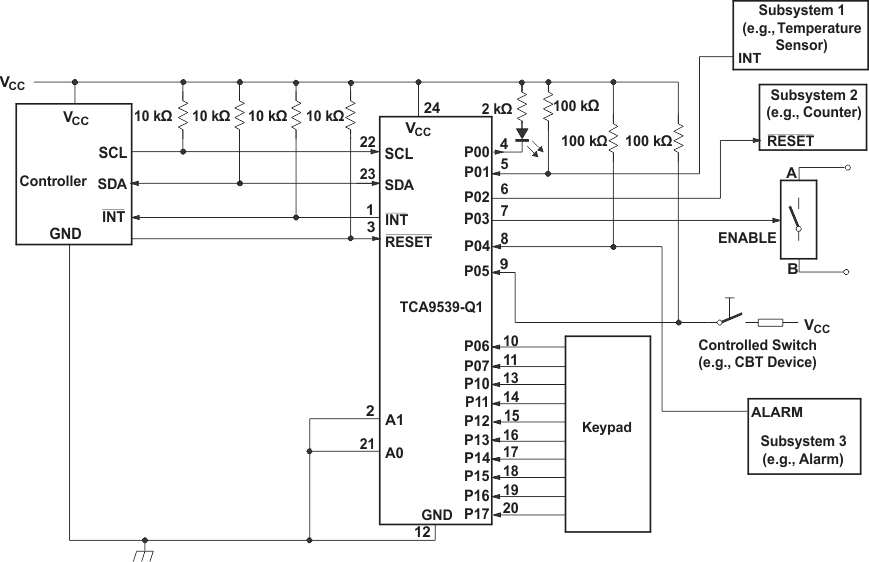
Figure 9-1 shows an application in which the TCA9539-Q1 can be used.
GUID-20210901-SS0I-VSSJ-VLX3-V7WZ4M9RLHNS-low.gif
Device address is configured as 1110100 for this example.
P00, P02, and P03 are configured as outputs.
P01 and P04 to P17 are configured as inputs.
Pin numbers shown are for the PW package.
Figure 9-1 Application Schematic