SCPS205B April   2014  – November 2019 TCA9546A

PRODUCTION DATA.  

  1. Features
  2. Applications
  3. Description
    1.     Device Images
      1.      Simplified Application Diagram
  4. Revision History
  5. Pin Configuration and Functions
    1.     Pin Functions
  6. Specifications
    1. 6.1 Absolute Maximum Ratings
    2. 6.2 ESD Ratings
    3. 6.3 Recommended Operating Conditions
    4. 6.4 Thermal Information
    5. 6.5 Electrical Characteristics
    6. 6.6 I2C Interface Timing Requirements
    7. 6.7 Switching Characteristics
    8. 6.8 Interrupt and Reset Timing Requirements
    9. 6.9 Typical Characteristics
  7. Parameter Measurement Information
  8. Detailed Description
    1. 8.1 Overview
    2. 8.2 Functional Block Diagram
    3. 8.3 Feature Description
    4. 8.4 Device Functional Modes
      1. 8.4.1 RESET Input
      2. 8.4.2 Power-On Reset
    5. 8.5 Programming
      1. 8.5.1 I2C Interface
    6. 8.6 Control Register
      1. 8.6.1 Device Address
      2. 8.6.2 Control Register Description
      3. 8.6.3 Control Register Definition
  9. Application and Implementation
    1. 9.1 Application Information
    2. 9.2 Typical Application
      1. 9.2.1 Design Requirements
      2. 9.2.2 Detailed Design Procedure
      3. 9.2.3 TCA9546A Application Curves
  10. 10Power Supply Recommendations
    1. 10.1 Power-On Reset Requirements
  11. 11Layout
    1. 11.1 Layout Guidelines
    2. 11.2 Layout Example
  12. 12Device and Documentation Support
    1. 12.1 Receiving Notification of Documentation Updates
    2. 12.2 Support Resources
    3. 12.3 Trademarks
    4. 12.4 Electrostatic Discharge Caution
    5. 12.5 Glossary
  13. 13Mechanical, Packaging, and Orderable Information

Package Options

Mechanical Data (Package|Pins)
Thermal pad, mechanical data (Package|Pins)
Orderable Information

Typical Application

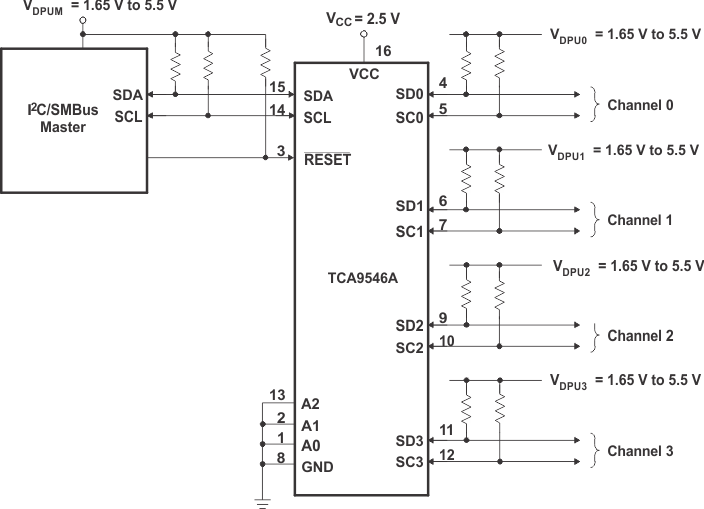
A typical application of the TCA9546A contains anywhere from 1 to 5 separate data pull-up voltages, VDPUX , one for the master device (VDPUM) and one for each of the selectable slave channels (VDPU0 – VDPU3). In the event where the master device and all slave devices operate at the same voltage, then the pass voltage, Vpass = VDPUX. Once the maximum Vpass is known, Vcc can be selected easily using Figure 16. In an application where voltage translation is necessary, additional design requirements must be considered (See Design Requirements).

Figure 15 shows an application in which the TCA9546A can be used.
TCA9546A typ_app_cps205.gifFigure 15. TCA9546A Typical Application Schematic