SCPS200E July 2009 – April 2019 TCA9555
PRODUCTION DATA.
- 1 Features
- 2 Applications
- 3 Description
- 4 Revision History
- 5 Description (continued)
- 6 Pin Configuration and Functions
- 7 Specifications
- 8 Parameter Measurement Information
- 9 Detailed Description
- 10Application and Implementation
- 11Power Supply Recommendations
- 12Layout
- 13Device and Documentation Support
- 14Mechanical, Packaging, and Orderable Information
Package Options
Mechanical Data (Package|Pins)
Thermal pad, mechanical data (Package|Pins)
Orderable Information
9.5.2.1.2 Reads
Reading from a slave is very similar to writing, but requires some additional steps. In order to read from a slave, the master must first instruct the slave which register it wishes to read from. This is done by the master starting off the transmission in a similar fashion as the write, by sending the address with the R/W bit equal to 0 (signifying a write), followed by the register address it wishes to read from. When the slave acknowledges this register address, the master sends a START condition again, followed by the slave address with the R/W bit set to 1 (signifying a read). This time, the slave acknowledges the read request, and the master releases the SDA bus but continues supplying the clock to the slave. During this part of the transaction, the master becomes the master-receiver, and the slave becomes the slave-transmitter.
The master continues to send out the clock pulses, but releases the SDA line so that the slave can transmit data. At the end of every byte of data, the master sends an ACK to the slave, letting the slave know that it is ready for more data. When the master has received the number of bytes it is expecting, it sends a NACK, signaling to the slave to halt communications and release the bus. The master follows this up with a STOP condition.
See the Control Register and Command Byte section to see list of the TCA9555's internal registers and a description of each one.
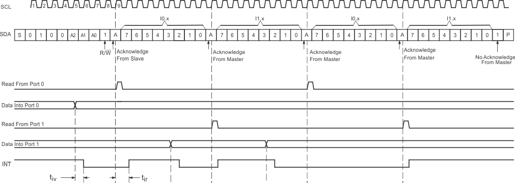
Figure 29 to Figure 31 show examples of reading a single byte from a slave register.
 Figure 29. Read from Register
 After a restart, the value of the register defined by the command byte matches the register being accessed when the restart occurred. For example, if the command byte references Input Port 1 before the restart, the restart occurs when Input Port 0 is being read. The original command byte is forgotten. If a subsequent restart occurs, Input Port 0 is read first. Data is clocked into the register on the rising edge of the ACK clock pulse. After the first byte is read, additional bytes may be read, but the data now reflect the information in the other register in the pair. For example, if Input Port 1 is read, the next byte read is Input Port 0.
Data is clocked into the register on the rising edge of the ACK clock pulse. There is no limitation on the number of data bytes received in one read transmission, but when the final byte is received, the bus master must not acknowledge the data.

