SCPS259E December   2014  – October 2024 TCA9617B

PRODUCTION DATA  

  1.   1
  2. Features
  3. Applications
  4. Description
  5. Pin Configuration and Functions
  6. Specifications
    1. 5.1 Absolute Maximum Ratings
    2. 5.2 ESD Ratings
    3. 5.3 Recommended Operating Conditions
    4. 5.4 Thermal Information
    5. 5.5 Electrical Characteristics
    6. 5.6 Timing Requirements
    7. 5.7 Typical Characteristics
  7.   Parameter Measurement Information
  8. Detailed Description
    1. 6.1 Overview
    2. 6.2 Functional Block Diagram
    3. 6.3 Feature Description
      1. 6.3.1 Bidirectional Level Translation
      2. 6.3.2 Low to High Transition Characteristics
      3. 6.3.3 High-to-Low Transition Characteristics
    4. 6.4 Device Functional Modes
  9. Application and Implementation
    1. 7.1 Application Information
    2. 7.2 Typical Application
      1. 7.2.1 Standard Application
        1. 7.2.1.1 Design Requirements
        2. 7.2.1.2 Detailed Design Procedure
          1. 7.2.1.2.1 Pullup Resistor Sizing
        3. 7.2.1.3 Application Curves
      2. 7.2.2 Star Application
        1. 7.2.2.1 Design Requirements
        2. 7.2.2.2 Detailed Design Procedure
        3. 7.2.2.3 Application Curves
      3. 7.2.3 Series Application
        1. 7.2.3.1 Design Requirements
        2. 7.2.3.2 Detailed Design Procedure
        3. 7.2.3.3 Application Curves
    3. 7.3 Power Supply Recommendations
    4. 7.4 Layout
      1. 7.4.1 Layout Guidelines
      2. 7.4.2 Layout Example
  10. Device and Documentation Support
    1. 8.1 Receiving Notification of Documentation Updates
    2. 8.2 Support Resources
    3. 8.3 Trademarks
    4. 8.4 Electrostatic Discharge Caution
    5. 8.5 Glossary
  11. Revision History
  12. 10Mechanical, Packaging, and Orderable Information
    1. 10.1 Tape and Reel Information

Package Options

Mechanical Data (Package|Pins)
Thermal pad, mechanical data (Package|Pins)
Orderable Information

Description

The TCA9617B is a BiCMOS dual bidirectional buffer intended for I2C bus and SMBus systems. The device provides bidirectional voltage-level translation (up-translation and down-translation) between low voltages (down to 0.8V) and higher voltages
(2.2V to 5.5V) in mixed-mode applications. This device enables I2C and similar bus systems to be extended, without degradation of performance even during level shifting.

The TCA9617B buffers both the serial data (SDA) and the serial clock (SCL) signals on the I2C bus, allowing two buses of 550pF to be connected in an I2C application. This device can also be used to separate two halves of a bus for voltage and capacitance.
Package Information
PART NUMBERPACKAGE(1)PACKAGE SIZE(2)
TCA9617BVSSOP (8)3mm × 3mm
For more information, see Section 10.
The package size (length × width) is a nominal value and includes pins, where applicable.
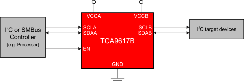
TCA9617B Simplified SchematicSimplified Schematic