SCPS259E December   2014  – October 2024 TCA9617B

PRODUCTION DATA  

  1.   1
  2. Features
  3. Applications
  4. Description
  5. Pin Configuration and Functions
  6. Specifications
    1. 5.1 Absolute Maximum Ratings
    2. 5.2 ESD Ratings
    3. 5.3 Recommended Operating Conditions
    4. 5.4 Thermal Information
    5. 5.5 Electrical Characteristics
    6. 5.6 Timing Requirements
    7. 5.7 Typical Characteristics
  7.   Parameter Measurement Information
  8. Detailed Description
    1. 6.1 Overview
    2. 6.2 Functional Block Diagram
    3. 6.3 Feature Description
      1. 6.3.1 Bidirectional Level Translation
      2. 6.3.2 Low to High Transition Characteristics
      3. 6.3.3 High-to-Low Transition Characteristics
    4. 6.4 Device Functional Modes
  9. Application and Implementation
    1. 7.1 Application Information
    2. 7.2 Typical Application
      1. 7.2.1 Standard Application
        1. 7.2.1.1 Design Requirements
        2. 7.2.1.2 Detailed Design Procedure
          1. 7.2.1.2.1 Pullup Resistor Sizing
        3. 7.2.1.3 Application Curves
      2. 7.2.2 Star Application
        1. 7.2.2.1 Design Requirements
        2. 7.2.2.2 Detailed Design Procedure
        3. 7.2.2.3 Application Curves
      3. 7.2.3 Series Application
        1. 7.2.3.1 Design Requirements
        2. 7.2.3.2 Detailed Design Procedure
        3. 7.2.3.3 Application Curves
    3. 7.3 Power Supply Recommendations
    4. 7.4 Layout
      1. 7.4.1 Layout Guidelines
      2. 7.4.2 Layout Example
  10. Device and Documentation Support
    1. 8.1 Receiving Notification of Documentation Updates
    2. 8.2 Support Resources
    3. 8.3 Trademarks
    4. 8.4 Electrostatic Discharge Caution
    5. 8.5 Glossary
  11. Revision History
  12. 10Mechanical, Packaging, and Orderable Information
    1. 10.1 Tape and Reel Information

Package Options

Mechanical Data (Package|Pins)
Thermal pad, mechanical data (Package|Pins)
Orderable Information

High-to-Low Transition Characteristics

When the A side of the bus is driven to 30% of VCCA, the B side driver turns on. This drives the B-side to 0V for a short period (see Figure 6-2), and then the B-side rises to the static offset voltage of 0.5V (VOL of TCA9617B). This effect, called an inverted pedestal, allows the B-side to drive to logic low much faster than driving to the static offset. Driving to the static offset voltage requires that the fall time be slowed to prevent ringing.
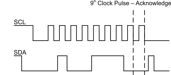
TCA9617B Bus A (0.8V to 5.5V Bus) WaveformFigure 6-1 Bus A (0.8V to 5.5V Bus) Waveform
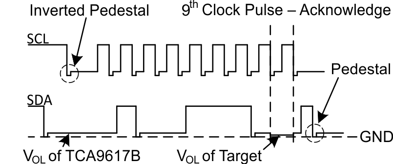
TCA9617B Bus B (2.2V to 5.5V Bus) WaveformFigure 6-2 Bus B (2.2V to 5.5V Bus) Waveform