SCPS265B March 2017 – February 2020 TCA9801
PRODUCTION DATA.
- 1 Features
- 2 Applications
- 3 Description
- 4 Revision History
- 5 Device Comparison Table
- 6 Pin Configuration and Functions
- 7 Specifications
- 8 Parameter Measurement Information
-
9 Detailed Description
- 9.1 Overview
- 9.2 Functional Block Diagram
- 9.3
Feature Description
- 9.3.1 Integrated Current Source
- 9.3.2 Ultra-Low Power Consumption
- 9.3.3 No Static-Voltage Offset
- 9.3.4 Active-High Repeater Enable Input
- 9.3.5 Powered Off High Impedance I2C Bus Pins on A-Side
- 9.3.6 Powered-Off Back-Power Protection for I2C Bus Pins
- 9.3.7 Clock Stretching and Multiple Master Arbitration Support
- 9.4 Device Functional Modes
- 10Application and Implementation
- 11Power Supply Recommendations
- 12Layout
- 13Device and Documentation Support
- 14Mechanical, Packaging, and Orderable Information
Package Options
Mechanical Data (Package|Pins)
- DGK|8
Thermal pad, mechanical data (Package|Pins)
Orderable Information
10.2.1.2 Detailed Design Procedure
Selection of the correct device is important for designers wanting optimize power consumption while transmitting.
Selecting the pull-up resistor required for the A-side is well documented already, see the I2C Bus Pullup Resistor Calculation application report. The rest of this section deals only with selection of a device based on the B-side design requirements.
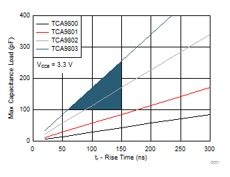
Since the B-ports of the TCA980x family have an integrated current source, the rise time is easily calculated with Equation 2. The graphs in the Application Curves section show the maximum capacitance load that each device can drive (based on minimum ICS value) to achieve a desired rise time, for different VCCB voltages.

The target design requirements example is intended for 400-kHz I2C, so the appropriate selection graph to use is Figure 22, and specifically Figure 27 since VCCB supply voltage is 3.3 V. In Figure 21, the graph has the appropriate regions shaded to help illustrate how to select the appropriate device. When looking at the general selection graphs, note that voltage line shifts evenly between the 1.65 V and 3.6 V traces in the general selection graphs. For example, if VCCB in another example is 2.5 V, then the selection graph is based on a line in the middle of the 1.65 V and the 3.6 V trace.
As shown in Figure 21, the shaded region is the appropriate region based on design requirements listed in Table 6. Any line that touches this shaded region is able to meet the design requirements. In this example, the TCA9803 and the TCA9802 both are able to satisfy the design requirements, since they both touch the shaded region. The TCA9800 and the TCA9801 both fall below the shaded region. While the TCA9801 is able to meet a rise time of about 190 ns at 100 pF (acceptable by the fast-mode rise time requirements), the design target in this example was ≤ 150 ns. This is a consideration a system designer can make, sacrificing rise time for a lower-power device, but in this example, the 150 ns limit is going to be upheld).
 Figure 21. Selection Guide Based on Example Design Requirements
 NOTE
Decoupling capacitors are not shown to keep the illustration simple. Decoupling capacitors (1 µF and 0.1 µF) must be placed close to each power supply pin.
Based on the selection graph shown above, the TCA9802 is selected, since it is the lowest-power device's trace (grey trace) which touches the shaded region. The TCA9803 may also be used without any consequences.