SCPS290A April 2024 – June 2024 TCAL6416R
PRODUCTION DATA
- 1
- 1 Features
- 2 Applications
- 3 Description
- 4 Pin Configuration and Functions
- 5 Specifications
- 6 Parameter Measurement Information
- 7 Detailed Description
- 8 Application and Implementation
- 9 Device and Documentation Support
- 10Revision History
- 11Mechanical, Packaging, and Orderable Information
Package Options
Refer to the PDF data sheet for device specific package drawings
Mechanical Data (Package|Pins)
- DTO|24
Thermal pad, mechanical data (Package|Pins)
Orderable Information
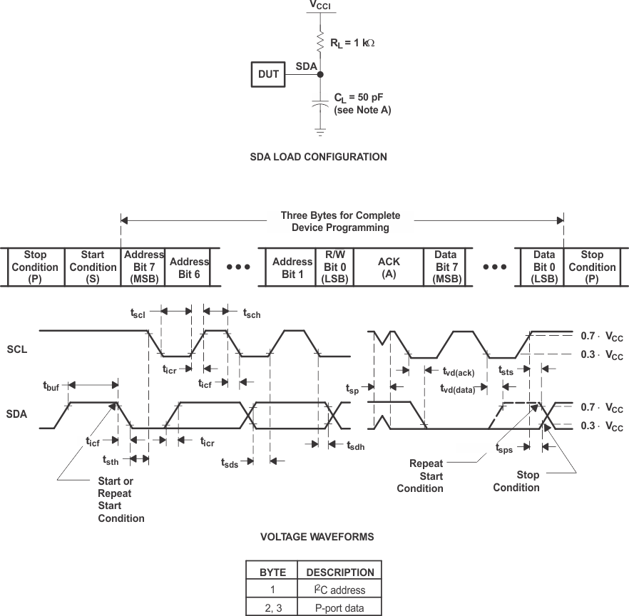
6 Parameter Measurement Information

A. CL includes probe and jig capacitance. tocf is measured with
CL of 10pF or 400pF.
B. All
inputs are supplied by generators having the following characteristics: PRR ≤ 10MHz, ZO = 50Ω, tr/tf ≤ 30ns.
C. All
parameters and waveforms are not applicable to all devices.
Figure 6-1 I2C Interface Load Circuit and Voltage Waveforms
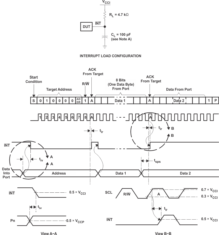
A. CL includes probe and
jig capacitance.
B. All inputs are supplied by
generators having the following characteristics: PRR ≤ 10MHz, ZO =
50Ω, tr/tf ≤ 30ns.
C. All parameters and waveforms are
not applicable to all devices.
Figure 6-2 Interrupt
Load Circuit and Voltage Waveforms
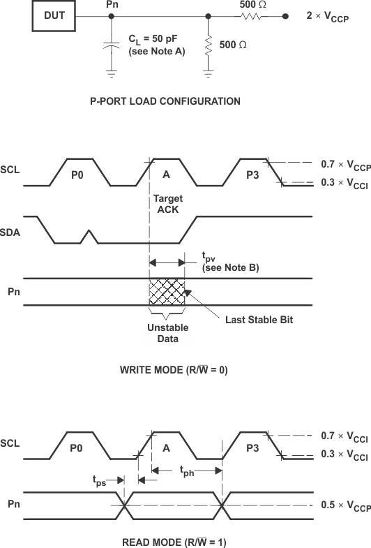
A. CL includes probe and
jig capacitance.
B. tpv is measured from
0.7 × VCC on SCL to 50% I/O (Pn) output.
C. All inputs are supplied by
generators having the following characteristics: PRR ≤ 10MHz, ZO =
50Ω, tr/tf ≤ 30ns.
D. The outputs are measured one at a
time, with one transition per measurement.
E. All parameters and waveforms are
not applicable to all devices.
Figure 6-3 P-Port
Load Circuit and Timing Waveforms
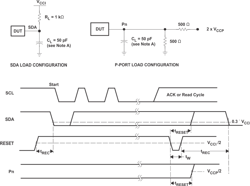
A. CL includes probe and
jig capacitance.
B. All inputs are supplied by
generators having the following characteristics: PRR ≤ 10MHz, ZO =
50Ω, tr/tf ≤ 30ns.
C. The outputs are measured one at a
time, with one transition per measurement.
D. I/Os are configured as
inputs.
E. All parameters and waveforms are
not applicable to all devices.
Figure 6-4 Reset
Load Circuits and Voltage Waveforms