SCPS280A November   2022  – November 2023 TCAL9538

PRODUCTION DATA  

  1.   1
  2. Features
  3. Applications
  4. Description
  5. Pin Configuration and Functions
  6. Specifications
    1. 5.1 Absolute Maximum Ratings
    2. 5.2 ESD Ratings
    3. 5.3 Recommended Operating Conditions
    4. 5.4 Thermal Information
    5. 5.5 Electrical Characteristics
    6. 5.6 Timing Requirements
    7. 5.7 I2C Bus Timing Requirements
    8. 5.8 Switching Characteristics
    9. 5.9 Typical Characteristics
  7. Parameter Measurement Information
  8. Detailed Description
    1. 7.1 Overview
    2. 7.2 Functional Block Diagrams
    3. 7.3 Feature Description
      1. 7.3.1 I/O Port
      2. 7.3.2 Adjustable Output Drive Strength
      3. 7.3.3 Interrupt Output (INT)
      4. 7.3.4 Reset Input (RESET)
      5. 7.3.5 Software Reset Call
    4. 7.4 Device Functional Modes
      1. 7.4.1 Power-On Reset
    5. 7.5 Programming
      1. 7.5.1 I2C Interface
    6. 7.6 Register Maps
      1. 7.6.1 Device Address
      2. 7.6.2 Control Register and Command Byte
      3. 7.6.3 Register Descriptions
      4. 7.6.4 Bus Transactions
        1. 7.6.4.1 Writes
        2. 7.6.4.2 Reads
  9. Application and Implementation
    1. 8.1 Application Information
    2. 8.2 Typical Application
      1. 8.2.1 Design Requirements
      2. 8.2.2 Detailed Design Procedure
        1. 8.2.2.1 Minimizing ICC When I/Os Control LEDs
      3. 8.2.3 Application Curves
    3. 8.3 Power Supply Recommendations
      1. 8.3.1 Power-On Reset Requirements
    4. 8.4 Layout
      1. 8.4.1 Layout Guidelines
      2. 8.4.2 Layout Example
  10. Device and Documentation Support
    1. 9.1 Receiving Notification of Documentation Updates
    2. 9.2 Support Resources
    3. 9.3 Trademarks
    4. 9.4 Electrostatic Discharge Caution
    5. 9.5 Glossary
  11. 10Revision History
  12. 11Mechanical, Packaging, and Orderable Information

Package Options

Refer to the PDF data sheet for device specific package drawings

Mechanical Data (Package|Pins)
  • PW|16
  • DTU|16
  • RSV|16
Thermal pad, mechanical data (Package|Pins)
Orderable Information

Reads

The bus controller first must send the TCAL9538 address with the LSB set to a logic 0 (see Figure 7-7 for device address). The command byte is sent after the address and determines which register is accessed.

Data is clocked into the register on the rising edge of the ACK clock pulse. There is no limitation on the number of data bytes received in one read transmission, but when the final byte is received, the bus controller must not acknowledge the data.

GUID-20220128-SS0I-NGNV-NJ0M-8CVBBKTHBSSJ-low.gif Figure 7-11 Read From Register

GUID-20220128-SS0I-KNCG-BKK7-NDRRQKVLXR46-low.gif
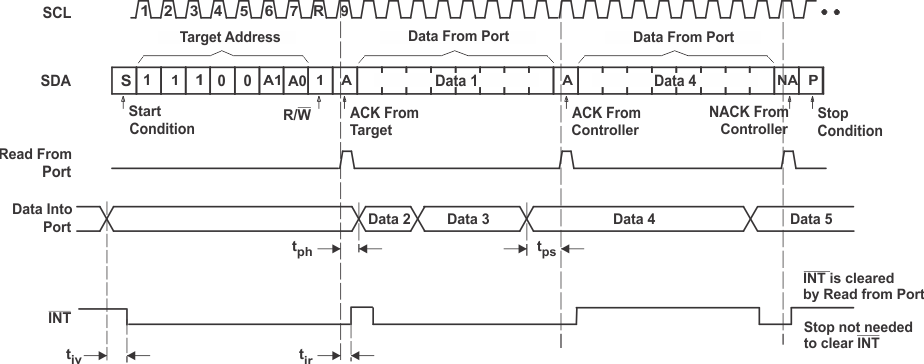
Transfer of data can be stopped at any time by a Stop condition. When this occurs, data present at the latest acknowledge phase is valid (output mode). It is assumed that the command byte previously has been set to 00 (read Input Port register).
This figure eliminates the command byte transfer, a restart, and target address call between the initial target address call and actual data transfer from P port (see Figure 7-11).
Figure 7-12 Read Input Port Register