SLLSFD1E January 2021 – March 2023 TCAN1043A-Q1
PRODUCTION DATA
- 1 Features
- 2 Applications
- 3 Description
- 4 Revision History
- 5 Pin Configuration and Functions
-
6 Specifications
- 6.1 Absolute Maximum Ratings
- 6.2 ESD Ratings
- 6.3 ESD Ratings - IEC Specifications
- 6.4 Recommended Operating Conditions
- 6.5 Thermal Information
- 6.6 Power Dissipation Ratings
- 6.7 Power Supply Characteristics
- 6.8 Electrical Characteristics
- 6.9 Timing Requirements
- 6.10 Switching Characteristics
- 6.11 Typical Characteristics
- 7 Parameter Measurement Information
-
8 Detailed Description
- 8.1 Overview
- 8.2 Functional Block Diagram
- 8.3
Feature Description
- 8.3.1 Supply Pins
- 8.3.2 Digital Inputs and Outputs
- 8.3.3 GND
- 8.3.4 INH Pin
- 8.3.5 WAKE Pin
- 8.3.6 CAN Bus Pins
- 8.3.7
Faults
- 8.3.7.1
Internal and External Fault Indicators
- 8.3.7.1.1 Power-Up (PWRON Flag)
- 8.3.7.1.2 Wake-Up Request (WAKERQ Flag)
- 8.3.7.1.3 Undervoltage Faults
- 8.3.7.1.4 CAN Bus Fault (CBF Flag)
- 8.3.7.1.5 TXD Clamped Low (TXDCLP Flag)
- 8.3.7.1.6 TXD Dominant State Timeout (TXDDTO Flag)
- 8.3.7.1.7 TXD Shorted to RXD Fault (TXDRXD Flag)
- 8.3.7.1.8 CAN Bus Dominant Fault (CANDOM Flag)
- 8.3.7.1
Internal and External Fault Indicators
- 8.3.8 Local Faults
- 8.4 Device Functional Modes
- 9 Application Information Disclaimer
- 10Power Supply Recommendations
- 11Layout
- 12Device and Documentation Support
- 13Mechanical, Packaging, and Orderable Information
Package Options
Mechanical Data (Package|Pins)
Thermal pad, mechanical data (Package|Pins)
- DMT|14
Orderable Information
8.3.8.2 TXD Dominant Timeout (TXD DTO)
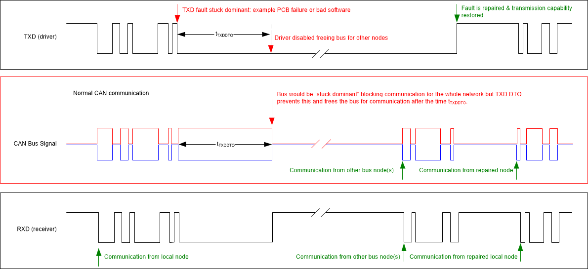
While the CAN driver is in active mode a TXD dominant state timeout circuit prevents the local node from blocking network communication in event of a hardware or software failure where TXD is held dominant longer than the timeout period, t > tTXDDTO. The TXD dominant state timeout circuit is triggered by a falling edge on the TXD pin. If no rising edge is seen before on TXD before t > tTXDDTO than the CAN driver is disabled releasing the bus lines to the recessive level. This keeps the bus free for communication between other nodes on the network.
The CAN driver will be activated again on the next dominant-to-recessive transition on the TXD pin. During a TXDDTO fault the high-speed receiver remains active and the RXD output pin will mirror the CAN bus.
 Figure 8-3 Timing Diagram for TXD DTO
The minimum dominant TXD time allowed by the dominant state timeout circuit limits the minimum possible transmitted data rate of the transceiver. The CAN protocol allows a maximum of eleven successive dominant bits to be transmitted in the worst case, where five successive dominant bits are followed immediately by an error frame. The minimum transmitted data rate may be calculated using the minimum tTXDDTO time in Equation 1.