SLLSEV0G November   2017  – December 2024 TCAN1043-Q1 , TCAN1043G-Q1 , TCAN1043H-Q1 , TCAN1043HG-Q1

PRODUCTION DATA  

  1.   1
  2. Features
  3. Applications
  4. Description
  5. Device Comparison Table
  6. Pin Configuration and Functions
  7. Specifications
    1. 6.1 Absolute Maximum Ratings
    2. 6.2 ESD Ratings
    3. 6.3 ESD Ratings IEC Specification
    4. 6.4 Recommended Operating Conditions
    5. 6.5 Thermal Information
    6. 6.6 Dissipation Ratings
    7. 6.7 Electrical Characteristics
    8. 6.8 Switching Characteristics
    9. 6.9 Typical Characteristics
  8. Parameter Measurement Information
  9. Detailed Description
    1. 8.1 Overview
    2. 8.2 Functional Block Diagram
    3. 8.3 Feature Description
      1. 8.3.1 Internal and External Indicator Flags (nFAULT and RXD)
      2. 8.3.2 Power-Up Flag (PWRON)
      3. 8.3.3 Wake-Up Request Flag (WAKERQ)
      4. 8.3.4 Wake-Up Source Recognition Flag (WAKESR)
      5. 8.3.5 Undervoltage Fault Flags
        1. 8.3.5.1 Undervoltage on VCC Fault
        2. 8.3.5.2 Undervoltage on VIO Fault
        3. 8.3.5.3 Undervoltage on VSUP Fault
      6. 8.3.6 CAN Bus Failure Fault Flag
      7. 8.3.7 Local Faults
        1. 8.3.7.1 TXD Dominant Timeout (TXD DTO)
        2. 8.3.7.2 TXD Shorted to RXD Fault
        3. 8.3.7.3 CAN Bus Dominant Fault
        4. 8.3.7.4 Thermal Shutdown (TSD)
        5. 8.3.7.5 RXD Recessive Fault
        6. 8.3.7.6 Undervoltage Lockout (UVLO)
        7. 8.3.7.7 Unpowered Device
        8. 8.3.7.8 Floating Terminals
        9. 8.3.7.9 CAN Bus Short Circuit Current Limiting
    4. 8.4 Device Functional Modes
      1. 8.4.1 CAN Bus States
      2. 8.4.2 Normal Mode
      3. 8.4.3 Silent Mode
      4. 8.4.4 Standby Mode
      5. 8.4.5 Go-to-Sleep Mode
      6. 8.4.6 Sleep Mode with Remote Wake and Local Wake Up Requests
        1. 8.4.6.1 Remote Wake Request via Wake Up Pattern (WUP)
        2. 8.4.6.2 Local Wake Up (LWU) via WAKE Input Terminal
      7. 8.4.7 Driver and Receiver Function Tables
      8. 8.4.8 Digital Inputs and Outputs
      9. 8.4.9 INH (Inhibit) Output
  10. Application Information Disclaimer
    1. 9.1 Application Information
    2. 9.2 Typical Application
      1. 9.2.1 Design Requirements
        1. 9.2.1.1 Bus Loading, Length and Number of Nodes
      2. 9.2.2 Detailed Design Procedures
        1. 9.2.2.1 CAN Termination
      3. 9.2.3 Application Curves
    3. 9.3 Power Supply Recommendations
    4. 9.4 Layout
      1. 9.4.1 Layout Guidelines
      2. 9.4.2 Layout Example
  11. 10Device and Documentation Support
    1. 10.1 Receiving Notification of Documentation Updates
    2. 10.2 Support Resources
    3. 10.3 Trademarks
    4. 10.4 Electrostatic Discharge Caution
    5. 10.5 Glossary
  12. 11Revision History
  13. 12Mechanical, Packaging, and Orderable Information
    1. 12.1 Mechanical, Packaging, and Orderable Information

Package Options

Refer to the PDF data sheet for device specific package drawings

Mechanical Data (Package|Pins)
  • D|14
  • DMT|14
Thermal pad, mechanical data (Package|Pins)
Orderable Information

CAN Bus States

The CAN bus has two logical states during operation: recessive and dominant. See Figure 8-2 and Figure 8-3.

In the recessive bus state the bus is biased to a common mode of approximately VCC/2 (2.5V) via the high resistance internal input resistors of the receiver of each node on the bus. Recessive is equivalent to a logic high and is typically a differential voltage on the bus of approximately 0V.

The dominant bus state is when the bus is driven differentially by one or more drivers. Current flows through the termination resistors and generates a differential voltage on the bus. Dominant is equivalent to a logic low and is a differential voltage on the bus greater than the minimum threshold for a CAN dominant. A dominant state overwrites the recessive state.

During arbitration, multiple CAN nodes may transmit a dominant bit at the same time. In this case, the differential voltage of the bus is greater than the differential voltage of a single driver.

The host microprocessor of the CAN node uses the TXD terminal to drive the bus and receives data from the bus on the RXD terminal.

The TCAN1043xx-Q1 transceivers has a third bus state in low power standby mode where the bus terminals are weakly biased to ground via the high resistance internal resistors of the receiver. See Figure 8-2 and Figure 8-3.
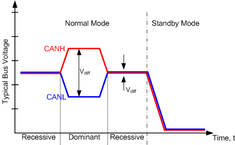
TCAN1043-Q1 TCAN1043H-Q1 TCAN1043HG-Q1 TCAN1043G-Q1 Bus States (Physical Bit Representation)Figure 8-2 Bus States (Physical Bit Representation)
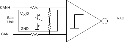
TCAN1043-Q1 TCAN1043H-Q1 TCAN1043HG-Q1 TCAN1043G-Q1 Bias Unit (Recessive Common Mode Bias) and Receiver
Normal and Silent Modes
Sleep and Standby Modes
Figure 8-3 Bias Unit (Recessive Common Mode Bias) and Receiver
TCAN1043-Q1 TCAN1043H-Q1 TCAN1043HG-Q1 TCAN1043G-Q1 State
                    Diagram
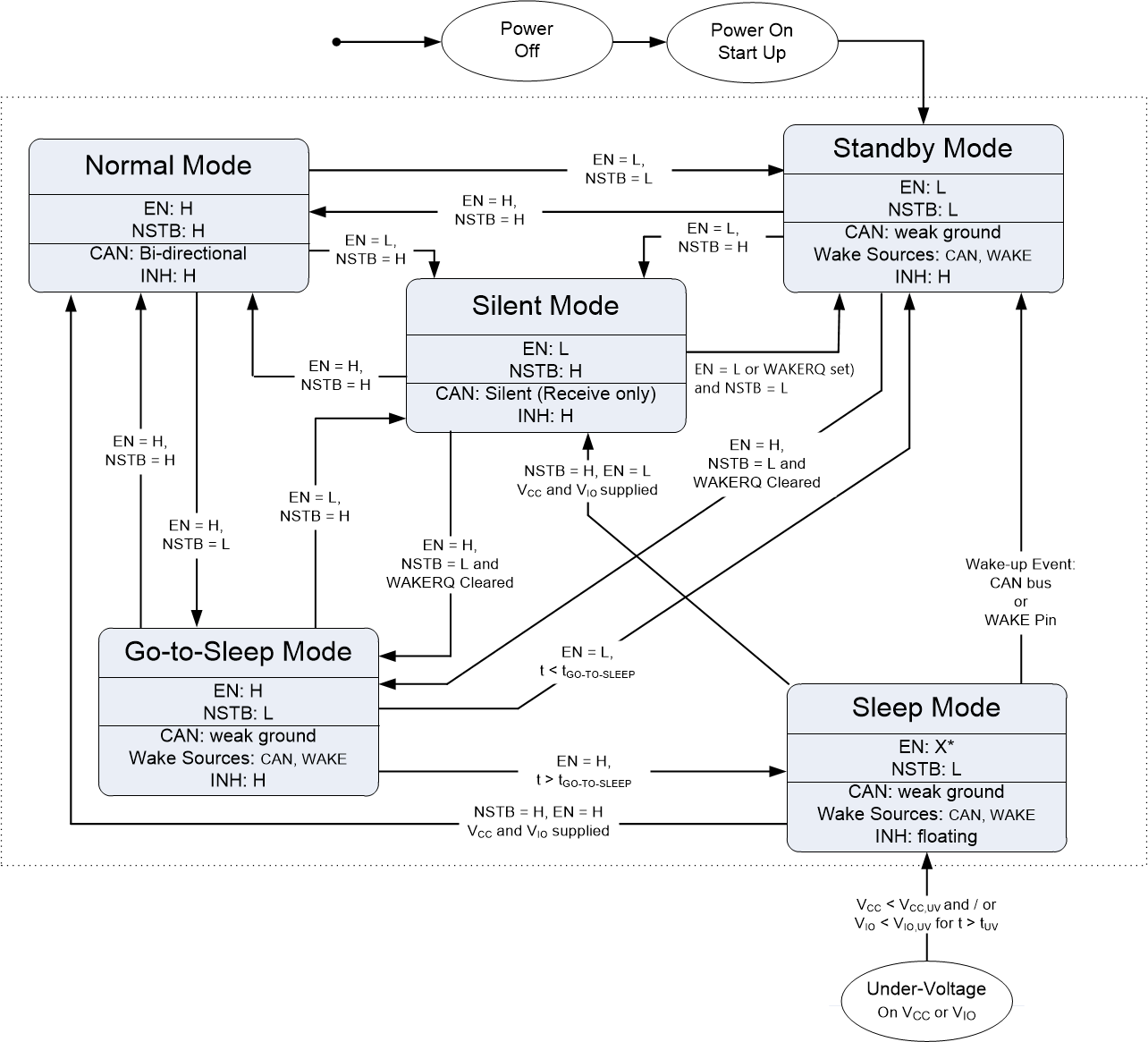
*The enable pin can be in a logical high or low state while in sleep mode. However, due to an internal pull-down, the lowest possible power consumption occurs when the pin is left either floating or pulled low externally.
Figure 8-4 State Diagram