SLLSEV0G November 2017 – December 2024 TCAN1043-Q1 , TCAN1043G-Q1 , TCAN1043H-Q1 , TCAN1043HG-Q1
PRODUCTION DATA
- 1
- 1 Features
- 2 Applications
- 3 Description
- 4 Device Comparison Table
- 5 Pin Configuration and Functions
- 6 Specifications
- 7 Parameter Measurement Information
-
8 Detailed Description
- 8.1 Overview
- 8.2 Functional Block Diagram
- 8.3 Feature Description
- 8.4 Device Functional Modes
- 9 Application Information Disclaimer
- 10Device and Documentation Support
- 11Revision History
- 12Mechanical, Packaging, and Orderable Information
Package Options
Refer to the PDF data sheet for device specific package drawings
Mechanical Data (Package|Pins)
- D|14
- DMT|14
Thermal pad, mechanical data (Package|Pins)
Orderable Information
8.4.6.1 Remote Wake Request via Wake Up Pattern (WUP)
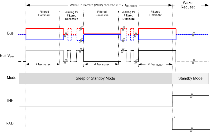
The TCAN1043xx-Q1 use the multiple filtered dominant wake up pattern (WUP) from ISO 11898-2 (2016) to qualify bus activity. The WUP is active for both sleep and standby modes, and results in the RXD terminal being driven low after a valid pattern is received.
The WUP consists of a filtered dominant pulse, followed by a filtered recessive pulse, and finally by a second filtered dominant pulse. The first filtered dominant initiates the WUP, and the bus monitor then waits on a filtered recessive. Other bus traffic does not reset the bus monitor. Once a filtered recessive is received, the bus monitor is waiting for a filtered dominant and again. Other bus traffic does not reset the bus monitor. Immediately upon reception of the second filtered dominant, the bus monitor recognizes the WUP and transition to standby mode, and drives the INH output high and sets the RXD terminal low (if VIO is present) to signal the wake up request.
For a dominant or recessive to be considered “filtered”, the bus must be in that state for more than the tWK_FILTER time. Due to variability in tWK_FILTER the following scenarios are applicable. Bus state times less than tWK_FILTER(MIN) are never detected as part of a WUP; thus, no wake request is generated. Bus state times between tWK_FILTER(MIN) and tWK_FILTER(MAX) may be detected as part of a WUP and a wake request may be generated. Bus state times greater than tWK_FILTER(MAX) are always detected as part of a WUP; thus, a wake request is always generated. See Figure 8-5 for the timing diagram of the WUP.
The pattern and tWK_FILTER time, used for the WUP and wake request, prevents noise and bus stuck dominant faults from causing false wake requests while allowing any CAN or CAN FD message to initiate a wake request.
If the device is switched to normal mode or an under voltage event occurs on either the VCC or VIO supplies, the wake request is lost.
ISO 11898-2 (2016) has two sets of times for a short and long wake up filter times. The tWK_FILTER timing for the TCAN1043xx-Q1 devices have been picked to be within the min and max values of both filter ranges. This timing has been chosen such that a single bit time at 500kbps, or two back to back bit times at 1Mbps triggers the filter in either bus state.

For an additional layer of robustness and to
prevent false wake-ups, the devices implement a timeout feature. For a remote wake
up event to successfully occur, the entire WUP must be received within the timeout
value
t < tWK_timeout (see Figure 8-5). If not, the internal logic is reset, and the part remains in the current state
without waking up. The full pattern must then be retransmitted, conforming to the
constraints mentioned in this section and shown in figure Figure 8-5.