SLLSF17C August   2019  – October 2024 TCAN1044-Q1

PRODUCTION DATA  

  1.   1
  2. Features
  3. Applications
  4. Description
  5. Pin Configuration and Functions
  6. Specifications
    1. 5.1  Absolute Maximum Ratings
    2. 5.2  ESD Ratings
    3. 5.3  ESD Ratings
    4. 5.4  Recommended Operating Conditions
    5. 5.5  Thermal Characteristics
    6. 5.6  Supply Characteristics
    7. 5.7  Dissipation Ratings
    8. 5.8  Electrical Characteristics
    9. 5.9  Switching Characteristics
    10. 5.10 Typical Characteristics
  7. Parameter Measurement Information
  8. Detailed Description
    1. 7.1 Overview
    2. 7.2 Functional Block Diagram
    3. 7.3 Feature Description
      1. 7.3.1 Pin Description
        1. 7.3.1.1 TXD
        2. 7.3.1.2 GND
        3. 7.3.1.3 VCC
        4. 7.3.1.4 RXD
        5. 7.3.1.5 VIO
        6. 7.3.1.6 CANH and CANL
        7. 7.3.1.7 STB (Standby)
      2. 7.3.2 CAN Bus States
      3. 7.3.3 TXD Dominant Timeout (DTO)
      4. 7.3.4 CAN Bus Short Circuit Current Limiting
      5. 7.3.5 Thermal Shutdown (TSD)
      6. 7.3.6 Undervoltage Lockout
      7. 7.3.7 Unpowered Device
      8. 7.3.8 Floating pins
    4. 7.4 Device Functional Modes
      1. 7.4.1 Operating Modes
      2. 7.4.2 Normal Mode
      3. 7.4.3 Standby Mode
        1. 7.4.3.1 Remote Wake Request via Wake-Up Pattern (WUP) in Standby Mode
      4. 7.4.4 Driver and Receiver Function
  9. Application and Implementation
    1. 8.1 Application Information
    2. 8.2 Typical Application
      1. 8.2.1 Design Requirements
        1. 8.2.1.1 CAN Termination
      2. 8.2.2 Detailed Design Procedures
        1. 8.2.2.1 Bus Loading, Length and Number of Nodes
      3. 8.2.3 Application Curves
    3. 8.3 System Examples
    4. 8.4 Power Supply Recommendations
    5. 8.5 Layout
      1. 8.5.1 Layout Guidelines
      2. 8.5.2 Layout Example
  10. Device and Documentation Support
    1. 9.1 Receiving Notification of Documentation Updates
    2. 9.2 Support Resources
    3. 9.3 Trademarks
    4. 9.4 Electrostatic Discharge Caution
    5. 9.5 Glossary
  11. 10Revision History
  12. 11Mechanical, Packaging, and Orderable Information

Package Options

Mechanical Data (Package|Pins)
Thermal pad, mechanical data (Package|Pins)
Orderable Information

Description

The TCAN1044-Q1 is a high speed controller area network (CAN) transceiver that meets the physical layer requirements of the ISO 11898-2:2016 high-speed CAN specification.

The TCAN1044-Q1 transceiver supports both classical CAN and CAN FD networks up to 8 megabits per second (Mbps). The TCAN1044-Q1 includes internal logic level translation via the VIO terminal to allow for interfacing the transceiver I/Os directly to 1.8V, 2.5V, 3.3V, or 5V logic I/Os. The transceiver supports a low-power standby mode and wake over CAN compliant to the ISO 11898-2:2016 defined wake-up pattern (WUP). The TCAN1044-Q1 transceiver also includes protection and diagnostic features supporting thermal-shutdown (TSD), TXD-dominant time-out (DTO), supply undervoltage detection, and bus fault protection up to ±58V.

Package Information
PART NUMBER PACKAGE(1) PACKAGE SIZE(2)
TCAN1044-Q1 SOT (DDF, 8) 2.9mm x 2.8mm
VSON (DRB, 8) 3mm x 3mm
SOIC (D, 8) 4.9mm x 6mm
For more information, see Section 11.
The package size (length × width) is a nominal value and includes pins, where applicable.
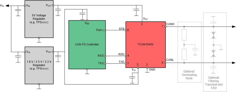
TCAN1044-Q1 Simplified Schematic Simplified Schematic