SLLSF18A March 2020 – September 2020 TCAN1046-Q1
PRODUCTION DATA
- 1 Features
- 2 Applications
- 3 Description
- 4 Revision History
- 5 Pin Configuration and Functions
- 6 Specifications
- 7 Parameter Measurement Information
-
8 Detailed Description
- 8.1 Overview
- 8.2 Functional Block Diagram
- 8.3 Feature Description
- 8.4 Device Functional Modes
- 9 Application and Implementation
- 10Power Supply Recommendations
- 11Layout
- 12Device and Documentation Support
- 13Mechanical, Packaging, and Orderable Information
Package Options
Mechanical Data (Package|Pins)
- DMT|14
Thermal pad, mechanical data (Package|Pins)
- DMT|14
Orderable Information
7 Parameter Measurement Information
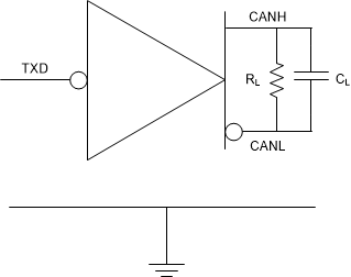
 Figure 7-1 ICC Test Circuit
 Figure 7-2 Driver Test Circuit and Measurement
 Figure 7-3 Receiver Test Circuit and Measurement
Table 7-1 Receiver Differential Input Voltage Threshold
Test
| Input (See Figure 7-3) | Output | |||
|---|---|---|---|---|
| VCANH | VCANL | |VID| | RXD | |
| -11.5 V | -12.5 V | 1000 mV | Low | VOL |
| 12.5 V | 11.5 V | 1000 mV | ||
| -8.55 V | -9.45 V | 900 mV | ||
| 9.45 V | 8.55 V | 900 mV | ||
| -8.75 V | -9.25 V | 500 mV | High | VOH |
| 9.25 V | 8.75 V | 500 mV | ||
| -11.8 V | -12.2 V | 400 mV | ||
| 12.2 V | 11.8 V | 400 mV | ||
| Open | Open | X | ||
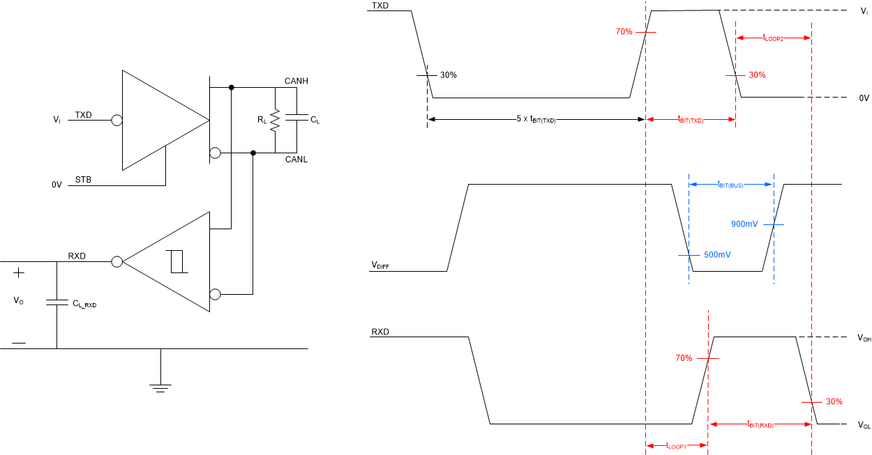
 Figure 7-4 Transmitter and Receiver Timing Test Circuit and
Measurement
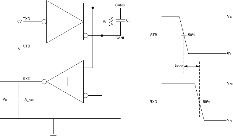
 Figure 7-5 tMODE Test Circuit and Measurement
 Figure 7-6 TXD
Dominant Timeout Test Circuit and
Measurement
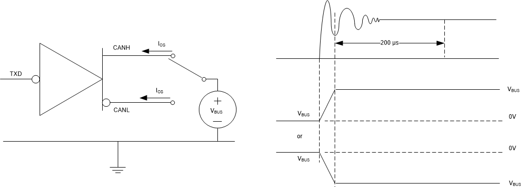
 Figure 7-7 Driver Short-Circuit Current Test and
Measurement