SLLSF70C September 2018 – February 2022 TCAN1046V-Q1
PRODUCTION DATA
- 1 Features
- 2 Applications
- 3 Description
- 4 Revision History
- 5 Pin Configuration and Functions
- 6 Specifications
- 7 Parameter Measurement Information
-
8 Detailed Description
- 8.1 Overview
- 8.2 Functional Block Diagram
- 8.3 Feature Description
- 8.4 Device Functional Modes
- 9 Application and Implementation
- 10Power Supply Recommendations
- 11Layout
- 12Device and Documentation Support
- 13Mechanical, Packaging, and Orderable Information
Package Options
Mechanical Data (Package|Pins)
- DMT|14
Thermal pad, mechanical data (Package|Pins)
- DMT|14
Orderable Information
3 Description
The TCAN1046V-Q1 is a dual, high-speed controller area network (CAN) transceiver that meets the physical layer requirements of the ISO 11898-2:2016 high-speed CAN specification.
The TCAN1046V-Q1 transceiver supports both classical CAN and CAN FD networks up to 8 megabits per second (Mbps). The TCAN1046V-Q1 includes internal logic level translation via the VIO terminal to allow for interfacing the transceiver IOs directly to 1.8 V, 2.5 V, 3.3 V, or 5 V logic IOs. The two CAN channels support independent mode control through the standby pins. This provides the ability to place each transceiver into its low-power state, standby mode, without impacting the state of the other CAN channel. While in standby mode the TCAN1046V-Q1 supports remote wake-up via the ISO 11898-2:2016 defined wake-up pattern (WUP). The TCAN1046V-Q1 transceivers also include many protection and diagnostic features including thermal shutdown (TSD), TXD dominant timeout (DTO), supply undervoltage detection, and bus fault protection up to ±58 V.
| PART NUMBER | PACKAGE(1) | BODY SIZE (NOM) |
|---|---|---|
| TCAN1046V-Q1 | VSON (14) | 4.50 mm x 3.00 mm |
| SOIC (14) | 8.95 mm x 3.91 mm |
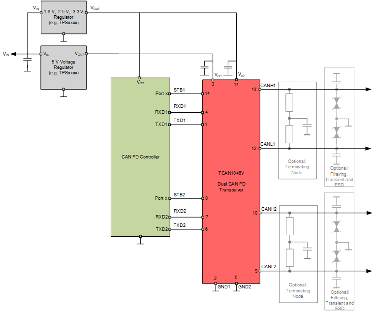
 Simplified Schematics