SLLSET0D March   2016  – April 2021 TCAN1051-Q1 , TCAN1051G-Q1 , TCAN1051GV-Q1 , TCAN1051H-Q1 , TCAN1051HG-Q1 , TCAN1051HGV-Q1 , TCAN1051HV-Q1 , TCAN1051V-Q1

PRODUCTION DATA  

  1. Features
  2. Applications
  3. Description
  4. Revision History
  5. Pin Configuration and Functions
  6. Specifications
    1. 6.1 Absolute Maximum Ratings
    2. 6.2 ESD Ratings
    3. 6.3 ESD Ratings, Specifications
    4. 6.4 Recommended Operating Conditions
    5. 6.5 Thermal Information
    6. 6.6 Power Rating
    7. 6.7 Electrical Characteristics
    8. 6.8 Switching Characteristics
    9. 6.9 Typical Characteristics
  7. Parameter Measurement Information
  8. Detailed Description
    1. 8.1 Overview
    2. 8.2 Functional Block Diagram
    3. 8.3 Feature Description
      1. 8.3.1 TXD Dominant Timeout (DTO)
      2. 8.3.2 Thermal Shutdown (TSD)
      3. 8.3.3 Undervoltage Lockout
      4. 8.3.4 Unpowered Device
      5. 8.3.5 Floating Terminals
      6. 8.3.6 CAN Bus Short Circuit Current Limiting
      7. 8.3.7 Digital Inputs and Outputs
        1. 8.3.7.1 5-V VCC Only Devices (Devices without the "V" Suffix):
        2. 8.3.7.2 5 V VCC with VIO I/O Level Shifting (Devices with the "V" Suffix):
    4. 8.4 Device Functional Modes
      1. 8.4.1 CAN Bus States
      2. 8.4.2 Normal Mode
      3. 8.4.3 Silent Mode
      4. 8.4.4 Driver and Receiver Function Tables
  9. Application Information Disclaimer
    1. 9.1 Application Information
    2. 9.2 Typical Applications
      1. 9.2.1 Design Requirements
        1. 9.2.1.1 Bus Loading, Length and Number of Nodes
      2. 9.2.2 Detailed Design Procedures
        1. 9.2.2.1 CAN Termination
      3. 9.2.3 Application Curves
  10. 10Power Supply Recommendations
  11. 11Device and Documentation Support
    1. 11.1 Documentation Support
      1. 11.1.1 Related Documentation
    2. 11.2 Receiving Notification of Documentation Updates
    3. 11.3 Support Resources
    4. 11.4 Trademarks
    5. 11.5 Electrostatic Discharge Caution
    6. 11.6 Glossary
  12. 12Mechanical, Packaging, and Orderable Information

Package Options

Mechanical Data (Package|Pins)
Thermal pad, mechanical data (Package|Pins)
Orderable Information

CAN Bus States

The CAN bus has two states during powered operation of the device: dominant and recessive. A dominant bus state is when the bus is driven differentially, corresponding to a logic low on the TXD and RXD terminal. A recessive bus state is when the bus is biased to VCC / 2 via the high-resistance internal input resistors RIN of the receiver, corresponding to a logic high on the TXD and RXD terminals.
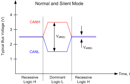
GUID-D1506BB2-FA8E-4C32-BDD9-D0CF46335BC5-low.gifFigure 8-2 Bus States (Physical Bit Representation)