SLLSFE3 December 2021 TCAN1164-Q1
PRODUCTION DATA
- 1 Features
- 2 Applications
- 3 Description
- 4 Revision History
- 5 Description (continued)
- 6 Device Comparison Table
- 7 Pin Configurations and Functions
- 8 Specifications
- 9 Parameter Measurement Information
-
10Detailed Description
- 10.1 Overview
- 10.2 Functional Block Diagram
- 10.3
Feature Description
- 10.3.1 VSUP Pin
- 10.3.2 VCCOUT Pin
- 10.3.3 Digital Inputs and Outputs
- 10.3.4 GND
- 10.3.5 nRST Pin
- 10.3.6 SDO
- 10.3.7 nCS Pin
- 10.3.8 SCLK
- 10.3.9 SDI
- 10.3.10 CAN Bus Pins
- 10.3.11 Local Faults
- 10.3.12 Watchdog
- 10.3.13 Bus Fault Detection and Communication
- 10.4 Device Functional Modes
- 10.5
Programming
- 10.5.1 Serial Peripheral Interface (SPI) Communication
- 10.5.2 Serial Clock Input (SCLK)
- 10.5.3 Serial Data Input (SDI)
- 10.5.4 Serial Data Output (SDO)
- 10.5.5 Chip Select Not (nCS)
- 10.5.6
Registers
- 10.5.6.1 DEVICE_ID_y Register (Address = 0h + formula) [reset = xxh]
- 10.5.6.2 REV_ID_MAJOR Register (Address = 8h) [reset = 00h]
- 10.5.6.3 REV_ID_MINOR Register (Address = 9h) [reset = 00h]
- 10.5.6.4 SPI_RSVD_x Register (Address = Ah + formula) [reset = 00h]
- 10.5.6.5 Scratch_Pad_SPI Register (Address = Fh) [reset = 00h]
- 10.5.6.6 MODE_CNTRL Register (Address = 10h) [reset = 04h]
- 10.5.6.7 WD_CONFIG_1 Register (Address = 13h) [reset = 54h]
- 10.5.6.8 WD_CONFIG_2 Register (Address = 14h) [reset = 02h]
- 10.5.6.9 WD_INPUT_TRIG Register (Address = 15h) [reset = 00h]
- 10.5.6.10 WD_QA_CONFIG Register (Address = 2Dh) [reset = 0h]
- 10.5.6.11 WD_QA_ANSWER Register (Address = 2Eh) [reset = 0h]
- 10.5.6.12 WD_QA_QUESTION Register (Address = 2Fh) [reset = 0h]
- 10.5.6.13 STATUS (address = 40h) [reset = 00h]
- 10.5.6.14 INT_GLOBAL Register (Address = 50h) [reset = 0h]
- 10.5.6.15 INT_1 Register (Address = 51h) [reset = 0h]
- 10.5.6.16 INT_2 Register (Address = 52h) [reset = 40h]
- 10.5.6.17 INT_3 Register (Address 53h) [reset = 0h]
- 10.5.6.18 INT_CANBUS Register (Address = 54h) [reset = 0h]
- 10.5.6.19 INT_ENABLE_1 Register (Address = 56h) [reset = F3h]
- 10.5.6.20 INT_ENABLE_2 Register (Address = 57h) [reset = 3Fh]
- 10.5.6.21 INT_ENABLE_3 Register (Address =58h) [reset = 80h]
- 10.5.6.22 INT_ENABLE_CANBUS Register (Address = 59h) [reset = 7Fh]
- 10.5.6.23 INT_RSVD_y Register (Address = 5Ah + formula) [reset = 00h]
- 11Application Information Disclaimer
- 12Power Supply Requirements
- 13Layout
- 14Device and Documentation Support
- 15Mechanical, Packaging, and Orderable Information
Package Options
Mechanical Data (Package|Pins)
- DMT|14
Thermal pad, mechanical data (Package|Pins)
- DMT|14
Orderable Information
10.3.11.1 TXD Dominant Timeout (TXD DTO)
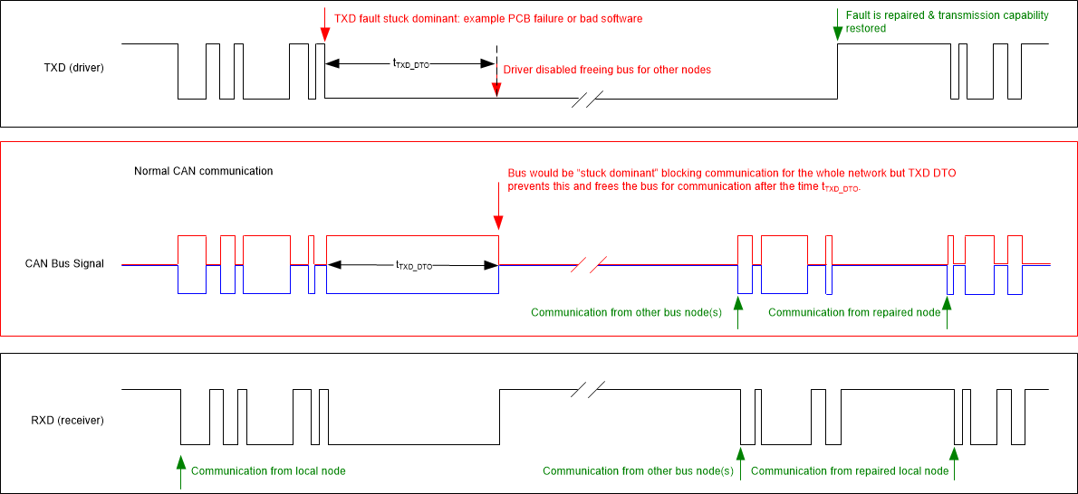
While the CAN driver is in active mode a TXD DTO circuit prevents the local node from blocking network communication in event of a hardware or software failure where TXD is held dominant longer than the time out period tTXD_DTO. The TXD DTO circuit is triggered by a falling edge on TXD. If no rising edge is seen before the time out constant of the circuit, tTXD_DTO, expires the CAN driver is disabled releasing the bus lines to the recessive level. This keeps the bus free for communication between other nodes on the network. The CAN driver is re-activated on the next dominant to recessive transition on the TXD terminal, thus clearing the dominant time out. The high-speed receiver and RXD terminal will reflect what is on the CAN bus during a TXD DTO fault. The TS terminal in driven low during a TXD DTO fault.
 Figure 10-3 Timing Diagram for TXD DTO
The minimum dominant TXD time allowed by the TXD DTO circuit limits the minimum possible transmitted data rate of the device. The CAN protocol allows a maximum of eleven successive dominant bits (on TXD) for the worst case, where five successive dominant bits are followed immediately by an error frame. The minimum transmitted data rate may be calculated using the minimum tTXD_DTO time and the maximum number of successive dominant bits (11 bits).