SLLSFF2B February 2022 – October 2024 TCAN1462-Q1
PRODUCTION DATA
- 1
- 1 Features
- 2 Applications
- 3 Description
- 4 Device Comparison Table
- 5 Pin Configurations and Functions
- 6 Specifications
- 7 Parameter Measurement Information
-
8 Detailed Description
- 8.1 Overview
- 8.2 Functional Block Diagram
- 8.3 Feature Description
- 8.4 Device Functional Modes
- 9 Application and Implementation
- 10Device and Documentation Support
- 11Revision History
- 12Mechanical, Packaging, and Orderable Information
Package Options
Mechanical Data (Package|Pins)
Thermal pad, mechanical data (Package|Pins)
- DRB|8
Orderable Information
8.1.1 Signal Improvement
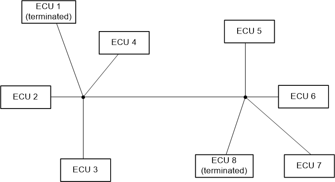
Signal improvement is an additional capability added to CAN FD transceiver that enhances the maximum data rate achievable in complex star topologies by minimizing signal ringing. Signal ringing is the result of reflections caused by impedance mismatch at various points in a CAN network due to the nodes that act as stubs.
An example of a complex network is shown in Figure 8-1.
 Figure 8-1 CAN Network: Star
topology
Figure 8-1 CAN Network: Star
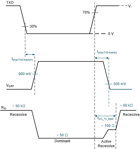
topologyRecessive-to-dominant signal edge is usually clean as it is strongly driven by the transmitter. Transmitter output impedance of CAN transceiver is ~50 Ω and matches to the network characteristic impedance. For a regular CAN FD transceiver, dominant-to-recessive edge is when the driver output impedance goes to ~60 kΩ and signal reflected back experiences impedance mismatch which causes ringing. TCAN1462-Q1 resolves this issue by TX-based Signal improvement capability (SIC). The device continues to drive the bus recessive until tSIC_TX_base so that reflections die down and recessive bit is clean at sampling point. In the active recessive phase, transmitter output impedance is low (~100 Ω). After this phase is over and device goes to passive recessive phase, driver output impedance goes to high-Z. This phenomenon is explained with Figure 8-2.
For more information on TI's signal improvement technology, and how it compares with similar devices in market, please refer to the white paper How Signal Improvement Capability Unlocks the Real Potential of CAN-FD Transceivers.
 Figure 8-2 TX based SIC