SLLSFP9 February 2024 TCAN1465-Q1 , TCAN1469-Q1
ADVANCE INFORMATION
- 1
- 1 Features
- 2 Applications
- 3 Description
- 4 Device Comparison Table
- 5 Pin Configuration and Functions
- 6 Specifications
- 7 Parameter Measurement Information
-
8 Detailed Description
- 8.1 Overview
- 8.2 Functional Block Diagram
- 8.3 Feature Description
- 8.4
Device Functional Modes
- 8.4.1 Normal Mode
- 8.4.2 Standby Mode
- 8.4.3 Listen Only Mode
- 8.4.4 Sleep Mode
- 8.4.5 Selective Wake-up
- 8.4.6 Fail-safe Features
- 8.4.7
Protection Features
- 8.4.7.1 Driver and Receiver Function
- 8.4.7.2 Floating Terminals
- 8.4.7.3 TXD Dominant Time Out (DTO)
- 8.4.7.4 CAN Bus Short Circuit Current Limiting
- 8.4.7.5 Thermal Shutdown
- 8.4.7.6 Under-Voltage Lockout (UVLO) and Unpowered Device
- 8.4.7.7
Watchdog (TCAN1469-Q1)
- 8.4.7.7.1 Watchdog Error Counter
- 8.4.7.7.2 Watchdog SPI Control Programming
- 8.4.7.7.3 Watchdog Timing
- 8.4.7.7.4 Question and Answer Watchdog
- 8.4.8 Bus Fault Detection and Communication (TCAN1469-Q1)
- 8.5 Programming
- 9 Application Information Disclaimer
-
10Registers
- 10.1
Register Maps
- 10.1.1 DEVICE_ID_y Register (Address = 0h + formula) [reset = value]
- 10.1.2 REV_ID_MAJOR Register (Address = 8h) [reset = 01h]
- 10.1.3 REV_ID_MINOR Register (Address = 9h) [reset = 00h]
- 10.1.4 SPI_RSVD_x Register (Address = Ah + formula) [reset = 00h]
- 10.1.5 Scratch_Pad_SPI Register (Address = Fh) [reset = 00h]
- 10.1.6 MODE_CNTRL Register (Address = 10h) [reset = 04h]
- 10.1.7 WAKE_PIN_CONFIG Register (Address = 11h) [reset = 4h]
- 10.1.8 PIN_CONFIG Register (Address = 12h) [reset = 00h]
- 10.1.9 WD_CONFIG_1 Register (Address = 13h) [reset = 15h]
- 10.1.10 WD_CONFIG_2 Register (Address = 14h) [reset = 02h]
- 10.1.11 WD_INPUT_TRIG Register (Address = 15h) [reset = 00h]
- 10.1.12 WD_RST_PULSE Register (Address = 16h) [reset = 07h]
- 10.1.13 FSM_CONFIG Register (Address = 17h) [reset = 00h]
- 10.1.14 FSM_CNTR Register (Address = 18h) [reset = 00h]
- 10.1.15 DEVICE_RST Register (Address = 19h) [reset = 00h]
- 10.1.16 DEVICE_CONFIG1 Register (Address = 1Ah) [reset = 00h]
- 10.1.17 DEVICE_CONFIG2 Register (Address = 1Bh) [reset = 0h]
- 10.1.18 SWE_EN Register (Address 1Ch) [reset = 04h]
- 10.1.19 SDO_CONFIG Register (Address = 29h) [reset = 00h]
- 10.1.20 WD_QA_CONFIG Register (Address = 2Dh) [reset = 00h]
- 10.1.21 WD_QA_ANSWER Register (Address = 2Eh) [reset = 00h]
- 10.1.22 WD_QA_QUESTION Register (Address = 2Fh) [reset = 3Ch]
- 10.1.23 SW_ID1 Register (Address = 30h) [reset = 00h]
- 10.1.24 SW_ID2 Register (Address = 31h) [reset = 00h]
- 10.1.25 SW_ID3 Register (Address = 32h) [reset = 00h]
- 10.1.26 SW_ID4 Register (Address = 33h) [reset = 00h]
- 10.1.27 SW_ID_MASK1 Register (Address = 34h) [reset = 00h]
- 10.1.28 SW_ID_MASK2 Register (Address = 35h) [reset = 00h]
- 10.1.29 SW_ID_MASK3 Register (Address = 36h) [reset = 00h]
- 10.1.30 SW_ID_MASK4 Register (Address = 37h) [reset = 00h]
- 10.1.31 SW_ID_MASK_DLC Register (Address = 38h) [reset = 00h]
- 10.1.32 DATA_y Register (Address = 39h + formula) [reset = 00h]
- 10.1.33 SW_RSVD_y Register (Address = 41h + formula) [reset = 00h]
- 10.1.34 SW_CONFIG_1 Register (Address = 44h) [reset = 50h]
- 10.1.35 SW_CONFIG_2 Register (Address = 45h) [reset = 00h]
- 10.1.36 SW_CONFIG_3 Register (Address = 46h) [reset = 1Fh]
- 10.1.37 SW_CONFIG_4 Register (Address = 47h) [reset = 00h]
- 10.1.38 SW_CONFIG_RSVD_y Register (Address = 48h + formula) [reset = 00h]
- 10.1.39 DEVICE_CONFIGx Register (Address = 4Bh) [reset = 0h]
- 10.1.40 INT_GLOBAL Register (Address = 50h) [reset = 00h]
- 10.1.41 INT_1 Register (Address = 51h) [reset = 00h]
- 10.1.42 INT_2 Register (Address = 52h) [reset = 40h]
- 10.1.43 INT_3 Register (Address 53h) [reset = 00h]
- 10.1.44 INT_CANBUS Register (Address = 54h) [reset = 00h]
- 10.1.45 INT_GLOBAL_ENABLE (Address = 55h) [reset = 00h]
- 10.1.46 INT_ENABLE_1 Register (Address = 56h) [reset = FFh]
- 10.1.47 INT_ENABLE_2 Register (Address = 57h) [reset = 1Fh]
- 10.1.48 INT_ENABLE_3 Register (Address = 58h) [reset = 0h]
- 10.1.49 INT_ENABLE_CANBUS Register (Address = 59h) [reset = 7Fh]
- 10.1.50 INT_RSVD_y Register (Address = 5Ah + formula) [reset = 00h]
- 10.1
Register Maps
- 11Device and Documentation Support
- 12Revision History
- 13Mechanical, Packaging, and Orderable Information
Package Options
Mechanical Data (Package|Pins)
Thermal pad, mechanical data (Package|Pins)
Orderable Information
8.4.5.6 WUF Data Validation
When the Data mask is enabled via the data mask bit, the data of the received frame must match the configured Data where at least one logic high (1) bit within the data field of the received frame matches a logic high (1) of the data field within the configured data. The relevant bit positions are determined by the configured Data in 8'h39 through 8'h40 and enabled by Data mask enable in 8'h38[0]. An example of a matching and non-matching Data is shown in Figure 8-20
 Figure 8-20 Data Field Validation for WUF Example
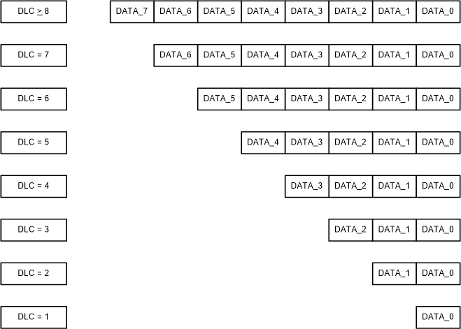
The selective wake data validation makes sure the last byte sent on the bus is interpreted as data mask byte 0. This means for 8 bytes of data, the first byte sent is interpreted as data mask byte 7. For a DLC of 3, the last byte sent on the bus is interpreted as data mask byte 0 and the first byte sent is interpreted as data mask byte 2. The following are a few examples of which bytes are used for various bytes sent and received.
 Figure 8-21 Data register mask values for different DLC values