SLLSFW8A June 2024 – December 2024 TCAN1472-Q1
PRODUCTION DATA
- 1
- 1 Features
- 2 Applications
- 3 Description
- 4 Pin Configurations and Functions
- 5 Specifications
- 6 Parameter Measurement Information
-
7 Detailed Description
- 7.1 Overview
- 7.2 Functional Block Diagram
- 7.3 Feature Description
- 7.4 Device Functional Modes
- 8 Application and Implementation
- 9 Device and Documentation Support
- 10Revision History
- 11Mechanical, Packaging, and Orderable Information
Package Options
Mechanical Data (Package|Pins)
Thermal pad, mechanical data (Package|Pins)
- DRB|8
Orderable Information
7.3.3 TXD Dominant Timeout (DTO)
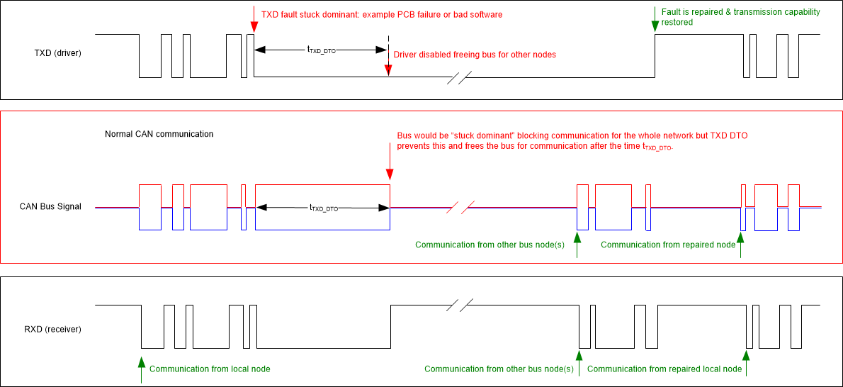
During normal mode, the only mode where the CAN driver is active, the TXD DTO circuit prevents the local node from blocking network communication in the event of a hardware or software failure where TXD is held dominant longer than the timeout period tTXD_DTO. The TXD DTO circuit is triggered by a falling edge on TXD. If no rising edge is seen before the timeout period of the circuit, tTXD_DTO, the CAN driver is disabled. Freeing the bus for communication between other nodes on the network. The CAN driver is reactivated when a recessive signal is seen on the TXD pin; thus, clearing the dominant time out. The receiver remains active and biased to VCC/2 and the RXD output reflects the activity on the CAN bus during the TXD DTO fault.
The minimum dominant TXD time allowed by the TXD DTO circuit limits the minimum possible transmitted data rate of the device. The CAN protocol allows a maximum of eleven successive dominant bits (on TXD) for the worst case, where five successive dominant bits are followed immediately by an error frame. The minimum transmitted data rate may be calculated using Equation 1.
 Figure 7-6 Example Timing Diagram for TXD
Dominant Timeout