SLLSF19 December 2017 TCAN4420
PRODUCTION DATA.
- 1 Features
- 2 Applications
- 3 Description
- 4 Revision History
- 5 Pin Configuration and Functions
- 6 Specifications
- 7 Parameter Measurement Information
- 8 Detailed Description
- 9 Application and Implementation
- 10Power Supply Recommendations
- 11Layout
- 12Device and Documentation Support
- 13Mechanical, Packaging, and Orderable Information
Package Options
Refer to the PDF data sheet for device specific package drawings
Mechanical Data (Package|Pins)
- D|8
Thermal pad, mechanical data (Package|Pins)
Orderable Information
7 Parameter Measurement Information
 Figure 6. Bus States (Physical Bit Representation)
 Figure 7. Common Mode Bias Unit and Receiver
 Figure 8. Supply Test Circuit
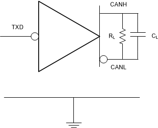
 Figure 9. Driver Test Circuit and Measurement
 Figure 10. Receiver Test Circuit and Measurement
 Figure 11. UV Re-enable Time after UV Event
 Figure 12. Transmitter and Receiver Timing Behavior Test Circuit and Measurement
 Figure 13. TXD_INT Dominant Time Out Test Circuit and Measurement
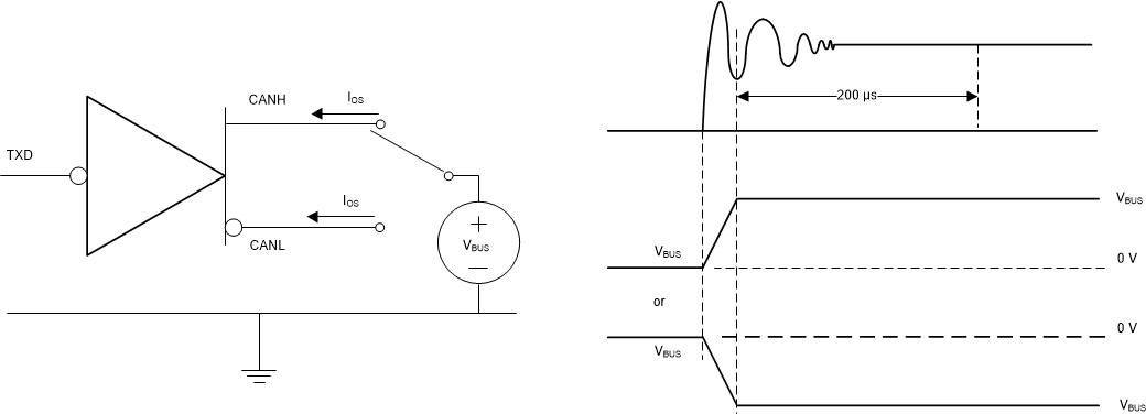
 Figure 14. Driver Short-Circuit Current Test and Measurement