SLLSF19 December   2017 TCAN4420

PRODUCTION DATA.  

  1. Features
  2. Applications
  3. Description
    1.     Device Images
      1.      Functional Block Diagram
  4. Revision History
  5. Pin Configuration and Functions
    1.     Pin Functions
  6. Specifications
    1. 6.1 Absolute Maximum Ratings
    2. 6.2 ESD Ratings
    3. 6.3 ESD Ratings Specifications
    4. 6.4 Recommended Operating Conditions
    5. 6.5 Thermal Information
    6. 6.6 Power Supply Characteristics
    7. 6.7 AC and DC Electrical Characteristics
    8. 6.8 Timing Requirements
    9. 6.9 Typical Characteristics
  7. Parameter Measurement Information
  8. Detailed Description
    1. 8.1 Overview
    2. 8.2 Functional Block Diagrams
    3. 8.3 Feature Description
      1. 8.3.1 TXD Dominant Time Out (DTO)
      2. 8.3.2 CAN Bus Short Circuit Current Limiting
      3. 8.3.3 Thermal Shutdown
      4. 8.3.4 Under Voltage Lockout (UVLO) and Unpowered Device
        1. 8.3.4.1 VIO Supply PIN
    4. 8.4 Device Functional Modes
      1. 8.4.1 Polarity Configuration
      2. 8.4.2 Normal Polarity Mode
      3. 8.4.3 Reverse Polarity Mode
      4. 8.4.4 Driver and Receiver Function
      5. 8.4.5 Floating Terminals
  9. Application and Implementation
    1. 9.1 Application Information
    2. 9.2 Typical Application
      1. 9.2.1 Design Requirements
        1. 9.2.1.1 Bus Loading, Length and Number of Nodes
      2. 9.2.2 Detailed Design Procedure
        1. 9.2.2.1 CAN Termination
      3. 9.2.3 Application Curves
  10. 10Power Supply Recommendations
  11. 11Layout
    1. 11.1 Layout Guidelines
    2. 11.2 Layout Example
  12. 12Device and Documentation Support
    1. 12.1 Device Support
      1. 12.1.1 Device Nomenclature
    2. 12.2 Receiving Notification of Documentation Updates
    3. 12.3 Community Resources
    4. 12.4 Trademarks
    5. 12.5 Electrostatic Discharge Caution
    6. 12.6 Glossary
  13. 13Mechanical, Packaging, and Orderable Information

Package Options

Refer to the PDF data sheet for device specific package drawings

Mechanical Data (Package|Pins)
  • D|8
Thermal pad, mechanical data (Package|Pins)
Orderable Information

Typical Characteristics

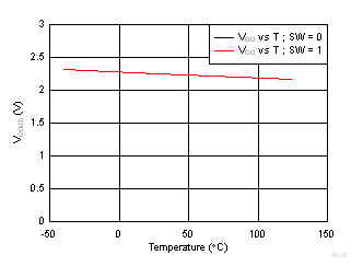
TCAN4420 SLLSF19_D001.gif
VCC = 5 V VIO = 5 V RL= 60Ω
CL = Open RCM = Open SW = 0 / 1
Figure 1. VOD(D) over Temperature
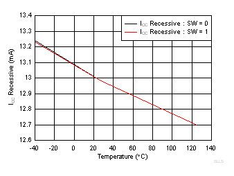
TCAN4420 SLLSF19_D003.gif
VCC = 5 V VIO = 5 V RL= 60Ω
CL = Open RCM = Open SW = 0 / 1
Figure 3. ICC over Temperature
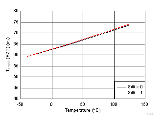
TCAN4420 SLLSF19_D008.gif
VCC = 5 V VIO = 5 V RL= 60 Ω
CL = Open RCM = Open SW = 0 / 1
Figure 5. Recessive to Dominant TLOOP vs Temperature
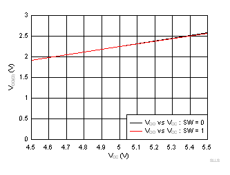
TCAN4420 SLLSF19_D002.gif
SW = 0 / 1 VIO = 5 V RL= 60Ω
CL = Open RCM = Open Temp = 25°C
Figure 2. VOD(D) over VCC Supply Voltage
TCAN4420 SLLSF19_D007.gif
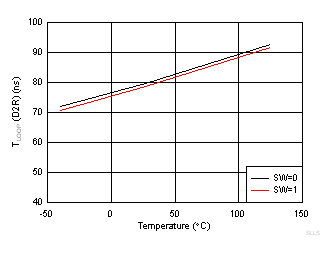
VCC = 5 V VIO = 5 V RL= 60Ω
CL = Open RCM = Open SW = 0 / 1
Figure 4. Dominant to Recessive TLOOP over Temperature