SPRS990F December 2016 – December 2018 TDA2P-ABZ
PRODUCTION DATA.
- 1Device Overview
- 2Revision History
- 3Device Comparison
-
4Terminal Configuration and Functions
- 4.1 Pin Diagram
- 4.2 Pin Attributes
- 4.3 Signal Descriptions
- 4.4 Pin Multiplexing
- 4.5 Connections for Unused Pins
-
5Specifications
- 5.1 Absolute Maximum Ratings
- 5.2 ESD Ratings
- 5.3 Power-On Hours (POH) Limits
- 5.4 Recommended Operating Conditions
- 5.5 Operating Performance Points
- 5.6 Power Consumption Summary
- 5.7
Electrical Characteristics
- Table 5-6 LVCMOS DDR DC Electrical Characteristics
- Table 5-7 Dual Voltage LVCMOS I2C DC Electrical Characteristics
- Table 5-8 IQ1833 Buffers DC Electrical Characteristics
- Table 5-9 IHHV1833 Buffers DC Electrical Characteristics
- Table 5-10 LVCMOS OSC Buffers DC Electrical Characteristics
- Table 5-11 BC1833IHHV Buffers DC Electrical Characteristics
- Table 5-12 Dual Voltage SDIO1833 DC Electrical Characteristics
- Table 5-13 Dual Voltage LVCMOS DC Electrical Characteristics
- 5.7.1 HDMIPHY DC Electrical Characteristics
- 5.7.2 SATAPHY DC Electrical Characteristics
- 5.7.3 USBPHY DC Electrical Characteristics
- 5.7.4 PCIEPHY DC Electrical Characteristics
- 5.8 VPP Specifications for One-Time Programmable (OTP) eFuses
- 5.9 Thermal Resistance Characteristics
- 5.10
Timing Requirements and Switching Characteristics
- 5.10.1 Timing Parameters and Information
- 5.10.2 Interface Clock Specifications
- 5.10.3 Power Supply Sequences
- 5.10.4 Clock Specifications
- 5.10.5 Recommended Clock and Control Signal Transition Behavior
- 5.10.6
Peripherals
- 5.10.6.1 Timing Test Conditions
- 5.10.6.2 Virtual and Manual I/O Timing Modes
- 5.10.6.3 VIP
- 5.10.6.4 DSS
- 5.10.6.5 HDMI
- 5.10.6.6 EMIF
- 5.10.6.7 GPMC
- 5.10.6.8 Timers
- 5.10.6.9 I2C
- 5.10.6.10 UART
- 5.10.6.11 McSPI
- 5.10.6.12 QSPI
- 5.10.6.13
McASP
- Table 5-74 Timing Requirements for McASP1
- Table 5-75 Timing Requirements for McASP2
- Table 5-76 Timing Requirements for McASP3/4/5/6/7/8
- Table 5-77 Switching Characteristics Over Recommended Operating Conditions for McASP1
- Table 5-78 Switching Characteristics Over Recommended Operating Conditions for McASP2
- Table 5-79 Switching Characteristics Over Recommended Operating Conditions for McASP3/4/5/6/7/8
- 5.10.6.14 USB
- 5.10.6.15 SATA
- 5.10.6.16 PCIe
- 5.10.6.17 CAN
- 5.10.6.18
GMAC_SW
- 5.10.6.18.1
GMAC MII Timings
- Table 5-96 Timing Requirements for miin_rxclk - MII Operation
- Table 5-97 Timing Requirements for miin_txclk - MII Operation
- Table 5-98 Timing Requirements for GMAC MIIn Receive 10/100 Mbit/s
- Table 5-99 Switching Characteristics Over Recommended Operating Conditions for GMAC MIIn Transmit 10/100 Mbits/s
- 5.10.6.18.2 GMAC MDIO Interface Timings
- 5.10.6.18.3
GMAC RMII Timings
- Table 5-104 Timing Requirements for GMAC REF_CLK - RMII Operation
- Table 5-105 Timing Requirements for GMAC RMIIn Receive
- Table 5-106 Switching Characteristics Over Recommended Operating Conditions for GMAC REF_CLK - RMII Operation
- Table 5-107 Switching Characteristics Over Recommended Operating Conditions for GMAC RMIIn Transmit 10/100 Mbits/s
- 5.10.6.18.4
GMAC RGMII Timings
- Table 5-111 Timing Requirements for rgmiin_rxc - RGMIIn Operation
- Table 5-112 Timing Requirements for GMAC RGMIIn Input Receive for 10/100/1000 Mbps
- Table 5-113 Switching Characteristics Over Recommended Operating Conditions for rgmiin_txctl - RGMIIn Operation for 10/100/1000 Mbit/s
- Table 5-114 Switching Characteristics for GMAC RGMIIn Output Transmit for 10/100/1000 Mbps
- 5.10.6.18.1
GMAC MII Timings
- 5.10.6.19
eMMC/SD/SDIO
- 5.10.6.19.1
MMC1—SD Card Interface
- 5.10.6.19.1.1 Default speed, 4-bit data, SDR, half-cycle
- 5.10.6.19.1.2 High speed, 4-bit data, SDR, half-cycle
- 5.10.6.19.1.3 SDR12, 4-bit data, half-cycle
- 5.10.6.19.1.4 SDR25, 4-bit data, half-cycle
- 5.10.6.19.1.5 UHS-I SDR50, 4-bit data, half-cycle
- 5.10.6.19.1.6 UHS-I SDR104, 4-bit data, half-cycle
- 5.10.6.19.1.7 UHS-I DDR50, 4-bit data
- 5.10.6.19.2 MMC2 — eMMC
- 5.10.6.19.3 MMC3 and MMC4—SDIO/SD
- 5.10.6.19.1
MMC1—SD Card Interface
- 5.10.6.20 GPIO
- 5.10.6.21 System and Miscellaneous interfaces
- 5.10.7
Emulation and Debug Subsystem
- 5.10.7.1
JTAG
- 5.10.7.1.1
JTAG Electrical Data/Timing
- Table 5-163 Timing Requirements for IEEE 1149.1 JTAG
- Table 5-164 Switching Characteristics Over Recommended Operating Conditions for IEEE 1149.1 JTAG
- Table 5-165 Timing Requirements for IEEE 1149.1 JTAG With RTCK
- Table 5-166 Switching Characteristics Over Recommended Operating Conditions for IEEE 1149.1 JTAG With RTCK
- 5.10.7.1.1
JTAG Electrical Data/Timing
- 5.10.7.2 Trace Port Interface Unit (TPIU)
- 5.10.7.1
JTAG
-
6Detailed Description
- 6.1 Description
- 6.2 Functional Block Diagram
- 6.3 MPU
- 6.4 DSP Subsystem
- 6.5 ISS
- 6.6 IVA
- 6.7 EVE
- 6.8 IPU
- 6.9 VPE
- 6.10 GPU
- 6.11 Memory Subsystem
- 6.12 Interprocessor Communication
- 6.13 Interrupt Controller
- 6.14 EDMA
- 6.15 Peripherals
- 6.16 On-Chip Debug
-
7Applications, Implementation, and Layout
- 7.1 Introduction
- 7.2 Power Optimizations
- 7.3 Core Power Domains
- 7.4 Single-Ended Interfaces
- 7.5
Differential Interfaces
- 7.5.1 General Routing Guidelines
- 7.5.2
USB 2.0 Board Design and Layout Guidelines
- 7.5.2.1 Background
- 7.5.2.2
USB PHY Layout Guide
- 7.5.2.2.1 General Routing and Placement
- 7.5.2.2.2
Specific Guidelines for USB PHY Layout
- 7.5.2.2.2.1 Analog, PLL, and Digital Power Supply Filtering
- 7.5.2.2.2.2 Analog, Digital, and PLL Partitioning
- 7.5.2.2.2.3 Board Stackup
- 7.5.2.2.2.4 Cable Connector Socket
- 7.5.2.2.2.5 Clock Routings
- 7.5.2.2.2.6 Crystals/Oscillator
- 7.5.2.2.2.7 DP/DM Trace
- 7.5.2.2.2.8 DP/DM Vias
- 7.5.2.2.2.9 Image Planes
- 7.5.2.2.2.10 JTAG Interface
- 7.5.2.2.2.11 Power Regulators
- 7.5.2.3 Electrostatic Discharge (ESD)
- 7.5.2.4 References
- 7.5.3 USB 3.0 Board Design and Layout Guidelines
- 7.5.4 HDMI Board Design and Layout Guidelines
- 7.5.5 SATA Board Design and Layout Guidelines
- 7.5.6 PCIe Board Design and Layout Guidelines
- 7.6 Clock Routing Guidelines
- 7.7
DDR2/DDR3 Board Design and Layout Guidelines
- 7.7.1 DDR2/DDR3 General Board Layout Guidelines
- 7.7.2 DDR2 Board Design and Layout Guidelines
- 7.7.3
DDR3 Board Design and Layout Guidelines
- 7.7.3.1 Board Designs
- 7.7.3.2 DDR3 EMIF
- 7.7.3.3 DDR3 Device Combinations
- 7.7.3.4 DDR3 Interface Schematic
- 7.7.3.5 Compatible JEDEC DDR3 Devices
- 7.7.3.6 PCB Stackup
- 7.7.3.7 Placement
- 7.7.3.8 DDR3 Keepout Region
- 7.7.3.9 Bulk Bypass Capacitors
- 7.7.3.10 High-Speed Bypass Capacitors
- 7.7.3.11 Net Classes
- 7.7.3.12 DDR3 Signal Termination
- 7.7.3.13 VREF_DDR Routing
- 7.7.3.14 VTT
- 7.7.3.15 CK and ADDR_CTRL Topologies and Routing Definition
- 7.7.3.16 Data Topologies and Routing Definition
- 7.7.3.17 Routing Specification
- 8Device and Documentation Support
- 9Mechanical Packaging Information
Package Options
Refer to the PDF data sheet for device specific package drawings
Mechanical Data (Package|Pins)
- ABZ|760
Thermal pad, mechanical data (Package|Pins)
Orderable Information
7.2.6.3.4 Guard Ring on PCB Edges
The major advantage of a multilayer PCB with ground-plane is the ground return path below each and every signal or power trace.
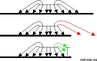
As shown in Figure 7-18 the field lines of the signal return to PCB ground as long as an infinite ground is available.
Traces near the PCB-edges do not have this infinite ground and therefore may radiate more than the others. Thus, signals (clocks) or power traces (core power) identified to be critical must not be routed in the vicinity of PCB edges, or, if not avoidable, must be accompanied by a guard ring on the PCB edge.
 Figure 7-18 Field Lines of a Signal Above Ground
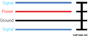
  Figure 7-19 Guard Ring Routing
 The intention of the guard ring is that HF-energy, that otherwise would have been emitted from the PCB edge, is reflected back into the board where it partially will be absorbed. For this purpose ground traces on the borders of all layers (including power layer) must be applied as shown in Figure 7-19.
As these traces must have the same (HF–) potential as the ground plane they must be connected to the ground plane at least every 10 mm.