SPRSP96A March 2024 – September 2024 TDA4AEN-Q1 , TDA4VEN-Q1
PRODUCTION DATA
- 1
- 1 Features
- 2 Applications
- 3 Description
- 4 Device Comparison
-
5 Terminal Configuration and Functions
- 5.1 Pin Diagrams
- 5.2 Pin Attributes
- 5.3
Signal Descriptions
- 13
- 5.3.1 CPSW3G
- 5.3.2 CPTS
- 5.3.3 CSI-2
- 5.3.4 DDRSS
- 5.3.5 DSI
- 5.3.6 DSS
- 5.3.7 ECAP
- 5.3.8 Emulation and Debug
- 5.3.9 EPWM
- 5.3.10 EQEP
- 5.3.11 GPIO
- 5.3.12 GPMC
- 5.3.13 I2C
- 5.3.14 MCAN
- 5.3.15 MCASP
- 5.3.16 MCSPI
- 5.3.17 MDIO
- 5.3.18 MMC
- 5.3.19 OLDI
- 5.3.20 OSPI
- 5.3.21 Power Supply
- 5.3.22 Reserved
- 5.3.23 SERDES
- 5.3.24 System and Miscellaneous
- 5.3.25 TIMER
- 5.3.26 UART
- 5.3.27 USB
- 5.4 Pin Connectivity Requirements
-
6 Specifications
- 6.1 Absolute Maximum Ratings
- 6.2 ESD Ratings for AEC - Q100 Qualified Devices in the AMW Package
- 6.3 Power-On Hours (POH)
- 6.4 Recommended Operating Conditions
- 6.5 Operating Performance Points
- 6.6
Electrical
Characteristics
- 6.6.1 I2C Open-Drain, and Fail-Safe (I2C OD FS) Electrical Characteristics
- 6.6.2 Fail-Safe Reset (FS RESET) Electrical Characteristics
- 6.6.3 High-Frequency Oscillator (HFOSC) Electrical Characteristics
- 6.6.4 Low-Frequency Oscillator (LFXOSC) Electrical Characteristics
- 6.6.5 SDIO Electrical Characteristics
- 6.6.6 LVCMOS Electrical Characteristics
- 6.6.7 CSI-2 (D-PHY) Electrical Characteristics
- 6.6.8 USB2PHY Electrical Characteristics
- 6.6.9 DDR Electrical Characteristics
- 6.7 VPP Specifications for One-Time Programmable (OTP) eFuses
- 6.8 Thermal Resistance Characteristics
- 6.9
Timing and Switching Characteristics
- 6.9.1 Timing Parameters and Information
- 6.9.2 Power Supply Requirements
- 6.9.3 System Timing
- 6.9.4 Clock Specifications
- 6.9.5
Peripherals
- 6.9.5.1 ATL
- 6.9.5.2 CPSW3G
- 6.9.5.3 CPTS
- 6.9.5.4 CSI-2
- 6.9.5.5 CSI-2 TX
- 6.9.5.6 DDRSS
- 6.9.5.7 DSS
- 6.9.5.8 ECAP
- 6.9.5.9 Emulation and Debug
- 6.9.5.10 EPWM
- 6.9.5.11 EQEP
- 6.9.5.12 GPIO
- 6.9.5.13 GPMC
- 6.9.5.14 I2C
- 6.9.5.15 MCAN
- 6.9.5.16 MCASP
- 6.9.5.17 MCSPI
- 6.9.5.18 MMCSD
- 6.9.5.19 OSPI
- 6.9.5.20 PCIe
- 6.9.5.21 Timers
- 6.9.5.22 UART
- 6.9.5.23 USB
- 7 Detailed Description
-
8 Applications,
Implementation, and Layout
- 8.1 Device Connection and Layout Fundamentals
- 8.2 Peripheral- and Interface-Specific Design Information
- 8.3 Clock Routing Guidelines
- 9 Device and Documentation Support
- 10Revision History
- 11Mechanical, Packaging, and Orderable Information
Package Options
Refer to the PDF data sheet for device specific package drawings
Mechanical Data (Package|Pins)
- AMW|594
Thermal pad, mechanical data (Package|Pins)
Orderable Information
6.9.3.1 Reset Timing
Tables and figures provided in this section define timing conditions, timing requirements, and switching characteristics for reset related signals.
Table 6-6 Reset Timing Conditions
| PARAMETER | MIN | MAX | UNIT | ||
|---|---|---|---|---|---|
| INPUT CONDITIONS | |||||
| SRI | Input slew rate | VDD(1) = 1.8V | 0.0018 | V/ns | |
| VDD(1) = 3.3V | 0.0033 | V/ns | |||
| OUTPUT CONDITIONS | |||||
| CL | Output load capacitance | 30 | pF | ||
(1) VDD stands for corresponding power supply. For more information on the power supply name and the corresponding ball(s), see POWER column of the Pin Attributes table.
Table 6-7 MCU_PORz Timing Requirements see Figure 6-7
| NO. | PARAMETER | MIN | MAX | UNIT | |
|---|---|---|---|---|---|
| RST1 | th(SUPPLIES_VALID - MCU_PORz) | Hold time, MCU_PORz active (low) at Power-up after supplies valid (using external crystal circuit) | 9500000 | ns | |
| RST2 | Hold time, MCU_PORz active (low) at Power-up after supplies valid and external clock stable (using external LVCMOS clock source) | 1200 | ns | ||
| RST3 | tw(MCU_PORzL) | Pulse Width, MCU_PORz low after Power-up (without removal of Power or system reference clock MCU_OSC0_XI/XO) | 1200 | ns | |
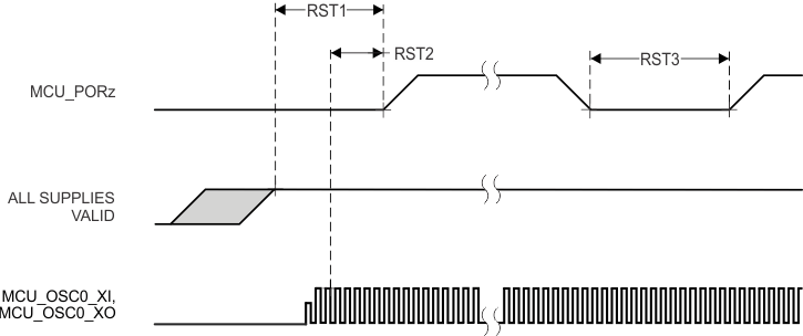 Figure 6-7 MCU_PORz Timing Requirements
 Table 6-8 MCU_RESETSTATz, and RESETSTATz Switching Characteristics see Figure 6-8
| NO. | PARAMETER | MIN | MAX | UNIT | |
|---|---|---|---|---|---|
| RST4 | td(MCU_PORzL-MCU_RESETSTATzL) | Delay time, MCU_PORz active (low) to MCU_RESETSTATz active (low) | 0 | ns | |
| RST5 | td(MCU_PORzH-MCU_RESETSTATzH) | Delay time, MCU_PORz inactive (high) to MCU_RESETSTATz inactive (high) | 6120*S(1) | ns | |
| RST6 | td(MCU_PORzL-RESETSTATzL) | Delay time, MCU_PORz active (low) to RESETSTATz active (low) | 0 | ns | |
| RST7 | td(MCU_PORzH-RESETSTATzH) | Delay time, MCU_PORz inactive (high) to RESETSTATz inactive (high) | 9195*S(1) | ns | |
| RST8 | tw(MCU_RESETSTATzL) | Pulse Width, MCU_RESETSTATz low (SW_MCU_WARMRST) | 966*S(1) | ns | |
| RST9 | tw(RESETSTATzL) | Pulse Width, RESETSTATz low (SW_MCU_WARMRST, SW_MAIN_PORz, or SW_MAIN_WARMRST) | 4040*S | ns | |
(1) S = MCU_OSC0_XI/XO clock period in ns.
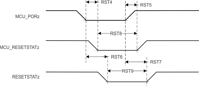 Figure 6-8 MCU_RESETSTATz, and RESETSTATz Switching Characteristics
Table 6-9 MCU_RESETz Timing Requirements see Figure 6-9
| NO. | PARAMETER | MIN | MAX | UNIT | |
|---|---|---|---|---|---|
| RST10 | tw(MCU_RESETzL)(1) | Pulse Width, MCU_RESETz active (low) | 1200 | ns | |
(1) This timing parameter is valid only after all supplies are valid and MCU_PORz has been asserted for the specified time.
Table 6-10 MCU_RESETSTATz, and RESETSTATz Switching Characteristics see Figure 6-9
| NO. | PARAMETER | MIN | MAX | UNIT | |
|---|---|---|---|---|---|
| RST11 | td(MCU_RESETzL-MCU_RESETSTATzL) | Delay time, MCU_RESETz active (low) to MCU_RESETSTATz active (low) | 0 | ns | |
| RST12 | td(MCU_RESETzH-MCU_RESETSTATzH) | Delay time, MCU_RESETz inactive (high) to MCU_RESETSTATz inactive (high) | 966*S(1) | ns | |
| RST13 | td(MCU_RESETzL-RESETSTATzL) | Delay time, MCU_RESETz active (low) to RESETSTATz active (low) | 960 | ns | |
| RST14 | td(MCU_RESETzH-RESETSTATzH) | Delay time, MCU_RESETz inactive (high) to RESETSTATz inactive (high) | 4040*S(1) | ns | |
(1) S = MCU_OSC0_XI/XO clock period in ns.
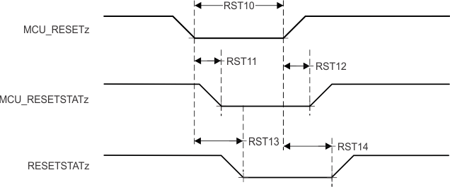 Figure 6-9 MCU_RESETz, MCU_RESETSTATz, and RESETSTATz Timing Requirements and Switching Characteristics
Table 6-11 RESET_REQz Timing Requirements see Figure 6-10
| NO. | PARAMETER | MIN | MAX | UNIT | |
|---|---|---|---|---|---|
| RST15 | tw(RESET_REQzL)(1) | Pulse Width, RESET_REQz active (low) | 1200 | ns | |
(1) This timing parameter is valid only after all supplies are valid and MCU_PORz has been asserted for the specified time.
Table 6-12 RESETSTATz Switching Characteristics see Figure 6-10
| NO. | PARAMETER | MIN | MAX | UNIT | |
|---|---|---|---|---|---|
| RST16 | td(RESET_REQzL-RESETSTATzL) | Delay time, RESET_REQz active (low) to RESETSTATz active (low) | 900*T(1) | ns | |
| RST17 | td(RESET_REQzH-RESETSTATzH) | Delay time, RESET_REQz inactive (high) to RESETSTATz inactive (high) | 4040*S(2) | ns | |
(1) T = Reset Isolation Time (Software Dependent)
(2) S = MCU_OSC0_XI/XO clock period in ns.
 Figure 6-10 RESET_REQz and RESETSTATz Timing Requirements and Switching Characteristics
Table 6-13 EMUx Timing Requirements see Figure 6-11
| NO. | PARAMETER | MIN | MAX | UNIT | |
|---|---|---|---|---|---|
| RST18 | tsu(EMUx-MCU_PORz) | Setup time, EMU[1:0] before MCU_PORz inactive (high) | 3*S(1) | ns | |
| RST19 | th(MCU_PORz - EMUx) | Hold time, EMU[1:0] after MCU_PORz inactive (high) | 10 | ns | |
(1) S = MCU_OSC0_XI/XO clock period in ns.
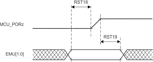 Figure 6-11 EMUx Timing Requirements
Table 6-14 BOOTMODE Timing Requirements see Figure 6-12
| NO. | PARAMETER | MIN | MAX | UNIT | |
|---|---|---|---|---|---|
| RST23 | tsu(BOOTMODE-PORz_OUT) | Setup time, BOOTMODE[15:00] valid before PORz_OUT high (External MCU PORz event or Software SW_MAIN_PORz) | 3*S(1) | ns | |
| RST24 | th(PORz_OUT - BOOTMODE) | Hold time, BOOTMODE[15:00] valid after PORz_OUT high (External MCU PORz event, or Software SW_MAIN_PORz) | 0 | ns | |
(1) S = MCU_OSC0_XI/XO clock period in ns.
Table 6-15 PORz_OUT Switching Characteristics see Figure 6-12
| NO. | PARAMETER | MIN | MAX | UNIT | |
|---|---|---|---|---|---|
| RST25 | td(MCU_PORzL-PORz_OUT) | Delay time, MCU_PORz active (low) to PORz_OUT active (low) | 0 | ns | |
| RST26 | td(MCU_PORzH-PORz_OUT) | Delay time, MCU_PORz inactive (high) to PORz_OUT inactive (high) | 1840 | ns | |
| RST27 | tw(PORz_OUTL) | Pulse Width, PORz_OUT low (MCU_PORz or SW_MAIN_PORz) | 1200 | ns | |
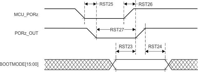 Figure 6-12 BOOTMODE Timing Requirements and PORz_OUT Switching Characteristics