SPRSP62B December   2022  – December 2024 TDA4AL-Q1 , TDA4VE-Q1 , TDA4VL-Q1

PRODUCTION DATA  

  1.   1
  2. Features
  3. Applications
  4. Description
    1. 3.1 Functional Block Diagram
  5. Device Comparison
  6. Terminal Configuration and Functions
    1. 5.1 Pin Diagrams
    2. 5.2 Pin Attributes
      1.      10
      2.      11
    3. 5.3 Signal Descriptions
      1.      13
      2. 5.3.1  ADC
        1. 5.3.1.1 MCU Domain
          1.        16
          2.        17
          3.        18
      3. 5.3.2  DDRSS
        1. 5.3.2.1 MAIN Domain
          1.        21
          2.        22
      4. 5.3.3  GPIO
        1. 5.3.3.1 MAIN Domain
          1.        25
        2. 5.3.3.2 WKUP Domain
          1.        27
      5. 5.3.4  I2C
        1. 5.3.4.1 MAIN Domain
          1.        30
          2.        31
          3.        32
          4.        33
          5.        34
          6.        35
          7.        36
        2. 5.3.4.2 MCU Domain
          1.        38
          2.        39
        3. 5.3.4.3 WKUP Domain
          1.        41
      6. 5.3.5  I3C
        1. 5.3.5.1 MCU Domain
          1.        44
      7. 5.3.6  MCAN
        1. 5.3.6.1 MAIN Domain
          1.        47
          2.        48
          3.        49
          4.        50
          5.        51
          6.        52
          7.        53
          8.        54
          9.        55
          10.        56
          11.        57
          12.        58
          13.        59
          14.        60
          15.        61
          16.        62
          17.        63
          18.        64
        2. 5.3.6.2 MCU Domain
          1.        66
          2.        67
      8. 5.3.7  MCSPI
        1. 5.3.7.1 MAIN Domain
          1.        70
          2.        71
          3.        72
          4.        73
          5.        74
          6.        75
          7.        76
        2. 5.3.7.2 MCU Domain
          1.        78
          2.        79
      9. 5.3.8  UART
        1. 5.3.8.1 MAIN Domain
          1.        82
          2.        83
          3.        84
          4.        85
          5.        86
          6.        87
          7.        88
          8.        89
          9.        90
          10.        91
        2. 5.3.8.2 MCU Domain
          1.        93
        3. 5.3.8.3 WKUP Domain
          1.        95
      10. 5.3.9  MDIO
        1. 5.3.9.1 MAIN Domain
          1.        98
        2. 5.3.9.2 MCU Domain
          1.        100
      11. 5.3.10 CPSW2G
        1. 5.3.10.1 MAIN Domain
          1.        103
        2. 5.3.10.2 MCU Domain
          1.        105
      12. 5.3.11 ECAP
        1. 5.3.11.1 MAIN Domain
          1.        108
          2.        109
          3.        110
      13. 5.3.12 EQEP
        1. 5.3.12.1 MAIN Domain
          1.        113
          2.        114
          3.        115
      14. 5.3.13 EPWM
        1. 5.3.13.1 MAIN Domain
          1.        118
          2.        119
          3.        120
          4.        121
          5.        122
          6.        123
          7.        124
      15. 5.3.14 USB
        1. 5.3.14.1 MAIN Domain
          1.        127
      16. 5.3.15 Display Port
        1. 5.3.15.1 MAIN Domain
          1.        130
      17. 5.3.16 Hyperlink
        1. 5.3.16.1 MAIN Domain
          1.        133
          2.        134
          3.        135
      18. 5.3.17 PCIE
        1. 5.3.17.1 MAIN Domain
          1.        138
      19. 5.3.18 SERDES
        1. 5.3.18.1 MAIN Domain
          1.        141
      20. 5.3.19 DSI
        1. 5.3.19.1 MAIN Domain
          1.        144
          2.        145
      21. 5.3.20 CSI
        1. 5.3.20.1 MAIN Domain
          1.        148
          2.        149
      22. 5.3.21 MCASP
        1. 5.3.21.1 MAIN Domain
          1.        152
          2.        153
          3.        154
          4.        155
          5.        156
      23. 5.3.22 DMTIMER
        1. 5.3.22.1 MAIN Domain
          1.        159
        2. 5.3.22.2 MCU Domain
          1.        161
      24. 5.3.23 CPTS
        1. 5.3.23.1 MAIN Domain
          1.        164
        2. 5.3.23.2 MCU Domain
          1.        166
      25. 5.3.24 DSS
        1. 5.3.24.1 MAIN Domain
          1.        169
      26. 5.3.25 GPMC
        1. 5.3.25.1 MAIN Domain
          1.        172
      27. 5.3.26 MMC
        1. 5.3.26.1 MAIN Domain
          1.        175
          2.        176
      28. 5.3.27 OSPI
        1. 5.3.27.1 MCU Domain
          1.        179
          2.        180
      29. 5.3.28 Hyperbus
        1. 5.3.28.1 MCU Domain
          1.        183
      30. 5.3.29 Emulation and Debug
        1. 5.3.29.1 MAIN Domain
          1.        186
          2.        187
      31. 5.3.30 System and Miscellaneous
        1. 5.3.30.1 Boot Mode configuration
          1.        190
        2. 5.3.30.2 Clock
          1.        192
          2.        193
        3. 5.3.30.3 System
          1.        195
          2.        196
        4. 5.3.30.4 EFUSE
          1.        198
        5. 5.3.30.5 VMON
          1.        200
      32. 5.3.31 Power
        1.       202
    4. 5.4 Connection for Unused Pins
  7. Specifications
    1. 6.1  Absolute Maximum Ratings
    2. 6.2  ESD Ratings
    3. 6.3  Recommended Operating Conditions
    4. 6.4  Power-On-Hour (POH) Limits
    5. 6.5  Operating Performance Points
    6. 6.6  Electrical Characteristics
      1. 6.6.1  I2C, Open-Drain, Fail-Safe (I2C OD FS) Electrical Characteristics
      2. 6.6.2  Fail-Safe Reset (FS Reset) Electrical Characteristics
      3. 6.6.3  HFOSC/LFOSC Electrical Characteristics
      4. 6.6.4  eMMCPHY Electrical Characteristics
      5. 6.6.5  SDIO Electrical Characteristics
      6. 6.6.6  CSI2/DSI D-PHY Electrical Characteristics
      7. 6.6.7  ADC12B Electrical Characteristics
      8. 6.6.8  LVCMOS Electrical Characteristics
      9. 6.6.9  USB2PHY Electrical Characteristics
      10. 6.6.10 SerDes 2-L-PHY/4-L-PHY Electrical Characteristics
      11. 6.6.11 UFS M-PHY Electrical Characteristics
      12. 6.6.12 eDP/DP AUX-PHY Electrical Characteristics
      13. 6.6.13 DDR0 Electrical Characteristics
    7. 6.7  VPP Specifications for One-Time Programmable (OTP) eFuses
      1. 6.7.1 Recommended Operating Conditions for OTP eFuse Programming
      2. 6.7.2 Hardware Requirements
      3. 6.7.3 Programming Sequence
      4. 6.7.4 Impact to Your Hardware Warranty
    8. 6.8  Thermal Resistance Characteristics
      1. 6.8.1 Thermal Resistance Characteristics for ALZ Package
    9. 6.9  Temperature Sensor Characteristics
    10. 6.10 Timing and Switching Characteristics
      1. 6.10.1 Timing Parameters and Information
      2. 6.10.2 Power Supply Sequencing
        1. 6.10.2.1 Power Supply Slew Rate Requirement
        2. 6.10.2.2 Combined MCU and Main Domains Power- Up Sequencing
        3. 6.10.2.3 Combined MCU and Main Domains Power- Down Sequencing
        4. 6.10.2.4 Isolated MCU and Main Domains Power- Up Sequencing
        5. 6.10.2.5 Isolated MCU and Main Domains Power- Down Sequencing
        6. 6.10.2.6 Independent MCU and Main Domains, Entry and Exit of MCU Only Sequencing
        7. 6.10.2.7 Independent MCU and Main Domains, Entry and Exit of DDR Retention State
        8. 6.10.2.8 Independent MCU and Main Domains, Entry and Exit of GPIO Retention Sequencing
      3. 6.10.3 System Timing
        1. 6.10.3.1 Reset Timing
        2. 6.10.3.2 Safety Signal Timing
        3. 6.10.3.3 Clock Timing
      4. 6.10.4 Clock Specifications
        1. 6.10.4.1 Input and Output Clocks / Oscillators
          1. 6.10.4.1.1 WKUP_OSC0 Internal Oscillator Clock Source
            1. 6.10.4.1.1.1 Load Capacitance
            2. 6.10.4.1.1.2 Shunt Capacitance
          2. 6.10.4.1.2 WKUP_OSC0 LVCMOS Digital Clock Source
          3. 6.10.4.1.3 Auxiliary OSC1 Internal Oscillator Clock Source
            1. 6.10.4.1.3.1 Load Capacitance
            2. 6.10.4.1.3.2 Shunt Capacitance
          4. 6.10.4.1.4 Auxiliary OSC1 LVCMOS Digital Clock Source
          5. 6.10.4.1.5 Auxiliary OSC1 Not Used
        2. 6.10.4.2 Output Clocks
        3. 6.10.4.3 PLLs
        4. 6.10.4.4 Module and Peripheral Clocks Frequencies
      5. 6.10.5 Peripherals
        1. 6.10.5.1  ATL
          1. 6.10.5.1.1 ATL_PCLK Timing Requirements
          2. 6.10.5.1.2 ATL_AWS[x] Timing Requirements
          3. 6.10.5.1.3 ATL_BWS[x] Timing Requirements
          4. 6.10.5.1.4 ATCLK[x] Switching Characteristics
        2. 6.10.5.2  CPSW2G
          1. 6.10.5.2.1 CPSW2G MDIO Interface Timings
          2. 6.10.5.2.2 CPSW2G RMII Timings
            1. 6.10.5.2.2.1 CPSW2G RMII[x]_REF_CLK Timing Requirements – RMII Mode
            2. 6.10.5.2.2.2 CPSW2G RMII[x]_RXD[1:0], RMII[x]_CRS_DV, and RMII[x]_RX_ER Timing Requirements – RMII Mode
            3. 6.10.5.2.2.3 CPSW2G RMII[x]_TXD[1:0], and RMII[x]_TX_EN Switching Characteristics – RMII Mode
          3. 6.10.5.2.3 CPSW2G RGMII Timings
            1. 6.10.5.2.3.1 RGMII[x]_RXC Timing Requirements – RGMII Mode
            2. 6.10.5.2.3.2 CPSW2G Timing Requirements for RGMII[x]_RD[3:0], and RGMII[x]_RCTL – RGMII Mode
            3. 6.10.5.2.3.3 CPSW2G RGMII[x]_TXC Switching Characteristics – RGMII Mode
            4. 6.10.5.2.3.4 RGMII[x]_TD[3:0], and RGMII[x]_TX_CTL Switching Characteristics – RGMII Mode
        3. 6.10.5.3  CSI-2
        4. 6.10.5.4  DDRSS
        5. 6.10.5.5  DSS
        6. 6.10.5.6  eCAP
          1. 6.10.5.6.1 Timing Requirements for eCAP
          2. 6.10.5.6.2 Switching Characteristics for eCAP
        7. 6.10.5.7  EPWM
          1. 6.10.5.7.1 Timing Requirements for eHRPWM
          2. 6.10.5.7.2 Switching Characteristics for eHRPWM
        8. 6.10.5.8  eQEP
          1. 6.10.5.8.1 Timing Requirements for eQEP
          2. 6.10.5.8.2 Switching Characteristics for eQEP
        9. 6.10.5.9  GPIO
          1. 6.10.5.9.1 GPIO Timing Requirements
          2. 6.10.5.9.2 GPIO Switching Characteristics
        10. 6.10.5.10 GPMC
          1. 6.10.5.10.1 GPMC and NOR Flash — Synchronous Mode
            1. 6.10.5.10.1.1 GPMC and NOR Flash Timing Requirements — Synchronous Mode
            2. 6.10.5.10.1.2 GPMC and NOR Flash Switching Characteristics – Synchronous Mode
          2. 6.10.5.10.2 GPMC and NOR Flash — Asynchronous Mode
            1. 6.10.5.10.2.1 GPMC and NOR Flash Timing Requirements – Asynchronous Mode
            2. 6.10.5.10.2.2 GPMC and NOR Flash Switching Characteristics – Asynchronous Mode
          3. 6.10.5.10.3 GPMC and NAND Flash — Asynchronous Mode
            1. 6.10.5.10.3.1 GPMC and NAND Flash Timing Requirements – Asynchronous Mode
            2. 6.10.5.10.3.2 GPMC and NAND Flash Switching Characteristics – Asynchronous Mode
          4. 6.10.5.10.4 GPMC0 IOSET
        11. 6.10.5.11 HyperBus
          1. 6.10.5.11.1 Timing Requirements for HyperBus
          2. 6.10.5.11.2 HyperBus 166 MHz Switching Characteristics
          3. 6.10.5.11.3 HyperBus 100 MHz Switching Characteristics
        12. 6.10.5.12 I2C
        13. 6.10.5.13 I3C
        14. 6.10.5.14 MCAN
        15. 6.10.5.15 MCASP
        16. 6.10.5.16 MCSPI
          1. 6.10.5.16.1 MCSPI — Controller Mode
          2. 6.10.5.16.2 MCSPI — Peripheral Mode
        17. 6.10.5.17 MMCSD
          1. 6.10.5.17.1 MMC0 - eMMC Interface
            1. 6.10.5.17.1.1 Legacy SDR Mode
            2. 6.10.5.17.1.2 High Speed SDR Mode
            3. 6.10.5.17.1.3 High Speed DDR Mode
            4. 6.10.5.17.1.4 HS200 Mode
            5. 6.10.5.17.1.5 HS400 Mode
          2. 6.10.5.17.2 MMC1/2 - SD/SDIO Interface
            1. 6.10.5.17.2.1 Default Speed Mode
            2. 6.10.5.17.2.2 High Speed Mode
            3. 6.10.5.17.2.3 UHS–I SDR12 Mode
            4. 6.10.5.17.2.4 UHS–I SDR25 Mode
            5. 6.10.5.17.2.5 UHS–I SDR50 Mode
            6. 6.10.5.17.2.6 UHS–I DDR50 Mode
            7. 6.10.5.17.2.7 UHS–I SDR104 Mode
        18. 6.10.5.18 CPTS
          1. 6.10.5.18.1 CPTS Timing Requirements
          2. 6.10.5.18.2 CPTS Switching Characteristics
        19. 6.10.5.19 OSPI
          1. 6.10.5.19.1 OSPI0/1 PHY Mode
            1. 6.10.5.19.1.1 OSPI0/1 With PHY Data Training
            2. 6.10.5.19.1.2 OSPI Without Data Training
              1. 6.10.5.19.1.2.1 OSPI Timing Requirements – SDR Mode
              2. 6.10.5.19.1.2.2 OSPI Switching Characteristics – SDR Mode
              3. 6.10.5.19.1.2.3 OSPI Timing Requirements – DDR Mode
              4. 6.10.5.19.1.2.4 OSPI Switching Characteristics – PHY DDR Mode
          2. 6.10.5.19.2 OSPI0/1 Tap Mode
            1. 6.10.5.19.2.1 OSPI0 Tap SDR Timing
            2. 6.10.5.19.2.2 OSPI0 Tap DDR Timing
        20. 6.10.5.20 PCIE
        21. 6.10.5.21 Timers
          1. 6.10.5.21.1 Timing Requirements for Timers
          2. 6.10.5.21.2 Switching Characteristics for Timers
        22. 6.10.5.22 UART
          1. 6.10.5.22.1 Timing Requirements for UART
          2. 6.10.5.22.2 UART Switching Characteristics
        23. 6.10.5.23 USB
      6. 6.10.6 Emulation and Debug
        1. 6.10.6.1 Trace
        2. 6.10.6.2 JTAG
          1. 6.10.6.2.1 JTAG Electrical Data and Timing
            1. 6.10.6.2.1.1 JTAG Timing Requirements
            2. 6.10.6.2.1.2 JTAG Switching Characteristics
  8. Applications, Implementation, and Layout
    1. 7.1 Device Connection and Layout Fundamentals
      1. 7.1.1 Power Supply Decoupling and Bulk Capacitors
        1. 7.1.1.1 Power Distribution Network Implementation Guidance
      2. 7.1.2 External Oscillator
      3. 7.1.3 JTAG and EMU
      4. 7.1.4 Reset
      5. 7.1.5 Unused Pins
      6. 7.1.6 Hardware Design Guide for JacintoTM 7 Devices
    2. 7.2 Peripheral- and Interface-Specific Design Information
      1. 7.2.1 LPDDR4 Board Design and Layout Guidelines
      2. 7.2.2 OSPI and QSPI Board Design and Layout Guidelines
        1. 7.2.2.1 No Loopback and Internal Pad Loopback
        2. 7.2.2.2 External Board Loopback
        3. 7.2.2.3 DQS (only available in Octal Flash devices)
      3. 7.2.3 USB VBUS Design Guidelines
      4. 7.2.4 System Power Supply Monitor Design Guidelines using VMON/POK
      5. 7.2.5 High Speed Differential Signal Routing Guidance
      6. 7.2.6 Thermal Solution Guidance
  9. Device and Documentation Support
    1. 8.1 Device Nomenclature
      1. 8.1.1 Standard Package Symbolization
      2. 8.1.2 Device Naming Convention
    2. 8.2 Tools and Software
    3. 8.3 Documentation Support
    4. 8.4 Trademarks
    5. 8.5 Support Resources
    6. 8.6 Electrostatic Discharge Caution
    7. 8.7 Glossary
  10. Revision History
  11. 10Mechanical, Packaging, and Orderable Information
    1. 10.1 Packaging Information

Package Options

Refer to the PDF data sheet for device specific package drawings

Mechanical Data (Package|Pins)
  • ALZ|770
Thermal pad, mechanical data (Package|Pins)
Orderable Information

MCSPI — Peripheral Mode

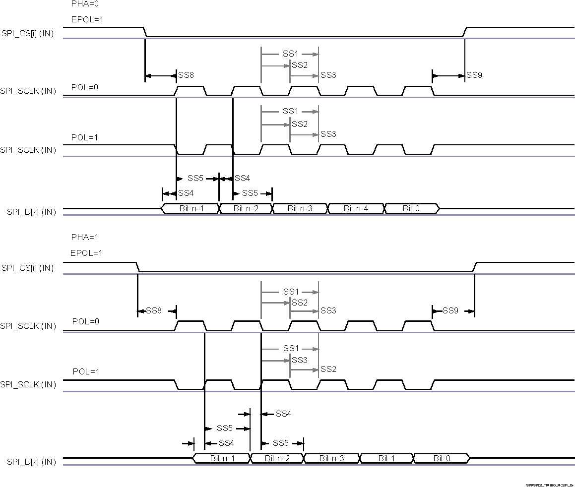
Table 6-53, Table 6-54, Figure 6-75, and Figure 6-76 present timing requirements and switching characteristics for MCSPI – Peripheral Mode.

Table 6-53 MCSPI Timing Requirements - Peripheral Mode
NO.PARAMETERDESCRIPTIONMODEMINMAXUNIT
SS1tc(spiclk)Cycle time, SPI_CLK20ns
SS2tw(spiclkL)Pulse duration, SPI_CLK low0.45P(1)ns
SS3tw(spiclkH)Pulse duration, SPI_CLK high0.45P(1)ns
SS4tsu(simoV-spiclkV)Setup time, SPI_D[x] valid before SPI_CLK active edge5ns
SS5th(spiclkV-simoV)Hold time, SPI_D[x] valid after SPI_CLK active edge5ns
SS8tsu(csV-spiclkV)Setup time, SPI_CSi valid before SPI_CLK first edge5ns
SS9th(spiclkV-csV)Hold time, SPI_CSi valid after SPI_CLK last edge5ns
Table 6-54 MCSPI Switching Characteristics - Peripheral Mode
NO.PARAMETERDESCRIPTIONMINMAXUNIT
SS6td(spiclkV-somiV)Delay time, SPI_CLK active edge to SPI_D[x] transition217.12ns
SS7tsk(csV-somiV)Delay time, SPI_CSi active edge to SPI_D[x] transition20.95ns
P = SPI_CLK period in ns.
TDA4VE-Q1 TDA4AL-Q1 TDA4VL-Q1 SPI Peripheral Mode
                                        Receive TimingFigure 6-75 SPI Peripheral Mode Receive Timing
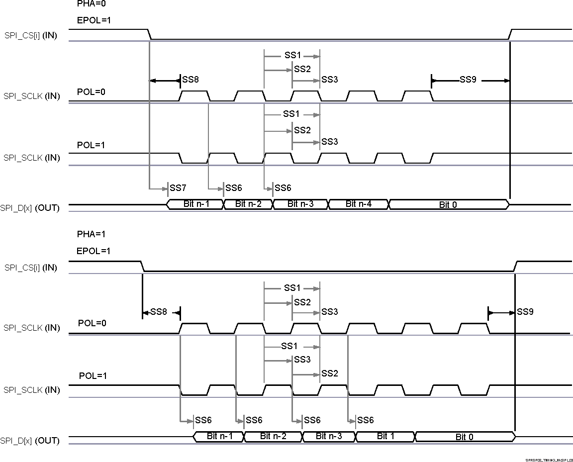
TDA4VE-Q1 TDA4AL-Q1 TDA4VL-Q1 MCSPI Peripheral Mode
                                        Transmit TimingFigure 6-76 MCSPI Peripheral Mode Transmit Timing

Table 6-55 and Table 6-56 present the specific groupings of signals (IOSET) for use with MCU_SPI0 and MCU_SPI1.

Table 6-55 MCU_SPI0 IOSETs
SignalsIOSET1IOSET2
BALL NAMEMUXBALL NAMEMUX
MCU_SPI0_CLKMCU_SPI0_CLK0MCU_SPI0_CLK0
MCU_SPI0_D0MCU_SPI0_D00MCU_SPI0_D00
MCU_SPI0_D1MCU_SPI0_D10MCU_SPI0_D10
MCU_SPI0_CS0MCU_SPI0_CS00MCU_SPI0_CS00
MCU_SPI0_CS1MCU_OSPI1_D35WKUP_GPIO0_121
MCU_SPI0_CS2MCU_OSPI1_CSn15WKUP_GPIO0_141
Table 6-56 MCU_SPI1 IOSET
SignalsIOSET1IOSET2
BALL NAMEMUXBALL NAMEMUX
MCU_SPI1_CLKMCU_SPI1_CLK0MCU_SPI1_CLK0
MCU_SPI1_D0MCU_SPI1_D00MCU_SPI1_D00
MCU_SPI1_D1MCU_SPI1_D10MCU_SPI1_D10
MCU_SPI1_CS0MCU_SPI1_CS00MCU_SPI1_CS00
MCU_SPI1_CS1MCU_OSPI1_D15WKUP_GPIO0_131
MCU_SPI1_CS2MCU_OSPI1_D25WKUP_GPIO0_151

For more information, see Multichannel Serial Peripheral Interface (MCSPI) section in Peripherals chapter in the device TRM.