SPRSPB4A June 2024 – December 2024 TDA4APE-Q1 , TDA4VPE-Q1
PRODUCTION DATA
- 1
- 1 Features
- 2 Applications
- 3 Description
- 4 Device Comparison
-
5 Terminal Configuration and Functions
- 5.1 Pin Diagrams
- 5.2 Pin Attributes
- 5.3
Signal Descriptions
- 13
- 5.3.1 ADC
- 5.3.2 CPSW2G
- 5.3.3 CPTS
- 5.3.4 CSI
- 5.3.5 DDRSS
- 5.3.6 Display Port
- 5.3.7 DMTIMER
- 5.3.8 DSI
- 5.3.9 DSS
- 5.3.10 ECAP
- 5.3.11 EPWM
- 5.3.12 EQEP
- 5.3.13 GPIO
- 5.3.14 GPMC
- 5.3.15 HYPERBUS
- 5.3.16 I2C
- 5.3.17 I3C
- 5.3.18 MCAN
- 5.3.19 MCASP
- 5.3.20 MCSPI
- 5.3.21 MDIO
- 5.3.22 MMC
- 5.3.23 OSPI
- 5.3.24 PCIE
- 5.3.25 SERDES
- 5.3.26 SGMII
- 5.3.27 UART
- 5.3.28 UFS
- 5.3.29 USB
- 5.3.30 Emulation and Debug
- 5.3.31 System and Miscellaneous
- 5.3.32 Power
- 5.4 Pin Connectivity Requirements
-
6 Specifications
- 6.1 Absolute Maximum Ratings
- 6.2 ESD Ratings
- 6.3 Power-On-Hour (POH) Limits
- 6.4 Recommended Operating Conditions
- 6.5 Operating Performance Points
- 6.6
Electrical Characteristics
- 6.6.1 I2C, Open-Drain, Fail-Safe (I2C OD FS) Electrical Characteristics
- 6.6.2 Fail-Safe Reset (FS Reset) Electrical Characteristics
- 6.6.3 HFOSC/LFOSC Electrical Characteristics
- 6.6.4 eMMCPHY Electrical Characteristics
- 6.6.5 SDIO Electrical Characteristics
- 6.6.6 CSI2/DSI D-PHY Electrical Characteristics
- 6.6.7 ADC12B Electrical Characteristics
- 6.6.8 LVCMOS Electrical Characteristics
- 6.6.9 USB2PHY Electrical Characteristics
- 6.6.10 SerDes 2-L-PHY/4-L-PHY Electrical Characteristics
- 6.6.11 UFS M-PHY Electrical Characteristics
- 6.6.12 eDP/DP AUX-PHY Electrical Characteristics
- 6.6.13 DDR0 Electrical Characteristics
- 6.7 VPP Specifications for One-Time Programmable (OTP) eFuses
- 6.8 Thermal Resistance Characteristics
- 6.9 Temperature Sensor Characteristics
- 6.10
Timing and Switching Characteristics
- 6.10.1 Timing Parameters and Information
- 6.10.2
Power Supply Sequencing
- 6.10.2.1 Power Supply Slew Rate Requirement
- 6.10.2.2 Combined MCU and Main Domains Power- Up Sequencing
- 6.10.2.3 Combined MCU and Main Domains Power- Down Sequencing
- 6.10.2.4 Isolated MCU and Main Domains Power- Up Sequencing
- 6.10.2.5 Isolated MCU and Main Domains Power- Down Sequencing
- 6.10.2.6 Independent MCU and Main Domains, Entry and Exit of MCU Only Sequencing
- 6.10.2.7 Independent MCU and Main Domains, Entry and Exit of DDR Retention State
- 6.10.2.8 Independent MCU and Main Domains, Entry and Exit of GPIO Retention Sequencing
- 6.10.3 System Timing
- 6.10.4
Clock Specifications
- 6.10.4.1 Input and Output Clocks / Oscillators
- 6.10.4.2 Output Clocks
- 6.10.4.3 PLLs
- 6.10.4.4 Module and Peripheral Clocks Frequencies
- 6.10.5
Peripherals
- 6.10.5.1 ATL
- 6.10.5.2
CPSW2G
- 6.10.5.2.1 CPSW2G MDIO Interface Timings
- 6.10.5.2.2 CPSW2G RMII Timings
- 6.10.5.2.3
CPSW2G RGMII Timings
- 6.10.5.2.3.1 RGMII[x]_RXC Timing Requirements – RGMII Mode
- 6.10.5.2.3.2 CPSW2G Timing Requirements for RGMII[x]_RD[3:0], and RGMII[x]_RCTL – RGMII Mode
- 6.10.5.2.3.3 CPSW2G RGMII[x]_TXC Switching Characteristics – RGMII Mode
- 6.10.5.2.3.4 RGMII[x]_TD[3:0], and RGMII[x]_TX_CTL Switching Characteristics – RGMII Mode
- 6.10.5.3 CSI-2
- 6.10.5.4 DDRSS
- 6.10.5.5 DSS
- 6.10.5.6 eCAP
- 6.10.5.7 EPWM
- 6.10.5.8 eQEP
- 6.10.5.9 GPIO
- 6.10.5.10 GPMC
- 6.10.5.11 HyperBus
- 6.10.5.12 I2C
- 6.10.5.13 I3C
- 6.10.5.14 MCAN
- 6.10.5.15 MCASP
- 6.10.5.16 MCSPI
- 6.10.5.17 MMCSD
- 6.10.5.18 CPTS
- 6.10.5.19 OSPI
- 6.10.5.20 OLDI
- 6.10.5.21 PCIE
- 6.10.5.22 Timers
- 6.10.5.23 UART
- 6.10.5.24 USB
- 6.10.6 Emulation and Debug
-
7 Applications,
Implementation, and Layout
- 7.1 Device Connection and Layout Fundamentals
- 7.2 Peripheral- and Interface-Specific Design Information
- 8 Device and Documentation Support
- 9 Revision History
- 10Mechanical, Packaging, and Orderable Information
Package Options
Refer to the PDF data sheet for device specific package drawings
Mechanical Data (Package|Pins)
- AND|1063
Thermal pad, mechanical data (Package|Pins)
Orderable Information
6.10.5.20.1 OLDI Switching Characteristics
| NO. | PARAMETER | MODE | MIN | MAX | UNIT |
|---|---|---|---|---|---|
| O1 | LVDS Low-to-High Transition Time max | IOSET1 | 0.18 | 0.5 | ns |
| O2 | LVDS high-to-low Transition Time max | IOSET1 | 0.18 | 0.5 | ns |
| O3 | Transmitter Output Bit Width min | IOSET1 | 1 | 1 | UI |
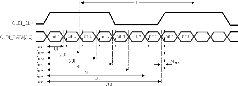
| O4 | Transmitter Pulse Positions – Normalized | IOSET1 | 0.25 | 0.75 | ns |
| O5 | Variation in transmitter pulse position across Bit 7:0 pulse positions | IOSET1 | -0.06 | 0.06 | ns |
| O6 | TxOut Channel to Channel Skew | IOSET1 | 110 | ns | |
| O7 | Transmitter Jitter Cycle-to-Cycle | IOSET1 | 0.028 | 0.035 | ns |
| O8 | Input Total Jitter Tolerance (Includes data to clock skew, pulse position variation.) | IOSET1 | 0.25 | ns |
 Figure 6-111 OLDI Transmitter Pulse Positions
 Figure 6-112 OLDI Data Output Jitter
 Figure 6-113 LVDS Output Transition Times
For more information, see Display Subsystem (DSS) and Peripherals section in Peripherals chapter in the device TRM.