SPRSP96A March   2024  – September 2024 TDA4AEN-Q1 , TDA4VEN-Q1

PRODUCTION DATA  

  1.   1
  2. Features
  3. Applications
  4. Description
    1. 3.1 Functional Block Diagram
  5. Device Comparison
  6. Terminal Configuration and Functions
    1. 5.1 Pin Diagrams
    2. 5.2 Pin Attributes
      1.      10
      2.      11
    3. 5.3 Signal Descriptions
      1.      13
      2. 5.3.1  CPSW3G
        1. 5.3.1.1 MAIN Domain
          1.        16
          2.        17
          3.        18
          4.        19
      3. 5.3.2  CPTS
        1. 5.3.2.1 MAIN Domain
          1.        22
      4. 5.3.3  CSI-2
        1. 5.3.3.1 MAIN Domain
          1.        25
          2.        26
          3.        27
          4.        28
      5. 5.3.4  DDRSS
        1. 5.3.4.1 MAIN Domain
          1.        31
      6. 5.3.5  DSI
        1. 5.3.5.1 MAIN Domain
          1.        34
      7. 5.3.6  DSS
        1. 5.3.6.1 MAIN Domain
          1.        37
      8. 5.3.7  ECAP
        1. 5.3.7.1 MAIN Domain
          1.        40
          2.        41
          3.        42
      9. 5.3.8  Emulation and Debug
        1. 5.3.8.1 MAIN Domain
          1.        45
        2. 5.3.8.2 MCU Domain
          1.        47
      10. 5.3.9  EPWM
        1. 5.3.9.1 MAIN Domain
          1.        50
          2.        51
          3.        52
          4.        53
      11. 5.3.10 EQEP
        1. 5.3.10.1 MAIN Domain
          1.        56
          2.        57
          3.        58
      12. 5.3.11 GPIO
        1. 5.3.11.1 MAIN Domain
          1.        61
          2.        62
        2. 5.3.11.2 MCU Domain
          1.        64
      13. 5.3.12 GPMC
        1. 5.3.12.1 MAIN Domain
          1.        67
      14. 5.3.13 I2C
        1. 5.3.13.1 MAIN Domain
          1.        70
          2.        71
          3.        72
          4.        73
          5.        74
        2. 5.3.13.2 MCU Domain
          1.        76
        3. 5.3.13.3 WKUP Domain
          1.        78
      15. 5.3.14 MCAN
        1. 5.3.14.1 MAIN Domain
          1.        81
          2.        82
        2. 5.3.14.2 MCU Domain
          1.        84
          2.        85
      16. 5.3.15 MCASP
        1. 5.3.15.1 MAIN Domain
          1.        88
          2.        89
          3.        90
          4.        91
          5.        92
      17. 5.3.16 MCSPI
        1. 5.3.16.1 MAIN Domain
          1.        95
          2.        96
          3.        97
        2. 5.3.16.2 MCU Domain
          1.        99
          2.        100
      18. 5.3.17 MDIO
        1. 5.3.17.1 MAIN Domain
          1.        103
      19. 5.3.18 MMC
        1. 5.3.18.1 MAIN Domain
          1.        106
          2.        107
          3.        108
      20. 5.3.19 OLDI
        1. 5.3.19.1 MAIN Domain
          1.        111
      21. 5.3.20 OSPI
        1. 5.3.20.1 MAIN Domain
          1.        114
      22. 5.3.21 Power Supply
        1.       116
      23. 5.3.22 Reserved
        1.       118
      24. 5.3.23 SERDES
        1. 5.3.23.1 MAIN Domain
          1.        121
          2.        122
          3.        123
      25. 5.3.24 System and Miscellaneous
        1. 5.3.24.1 Boot Mode Configuration
          1. 5.3.24.1.1 MAIN Domain
            1.         127
        2. 5.3.24.2 Clock
          1. 5.3.24.2.1 MCU Domain
            1.         130
          2. 5.3.24.2.2 WKUP Domain
            1.         132
        3. 5.3.24.3 System
          1. 5.3.24.3.1 MAIN Domain
            1.         135
          2. 5.3.24.3.2 MCU Domain
            1.         137
          3. 5.3.24.3.3 WKUP Domain
            1.         139
        4. 5.3.24.4 VMON
          1.        141
      26. 5.3.25 TIMER
        1. 5.3.25.1 MAIN Domain
          1.        144
        2. 5.3.25.2 MCU Domain
          1.        146
        3. 5.3.25.3 WKUP Domain
          1.        148
      27. 5.3.26 UART
        1. 5.3.26.1 MAIN Domain
          1.        151
          2.        152
          3.        153
          4.        154
          5.        155
          6.        156
          7.        157
        2. 5.3.26.2 MCU Domain
          1.        159
        3. 5.3.26.3 WKUP Domain
          1.        161
      28. 5.3.27 USB
        1. 5.3.27.1 MAIN Domain
          1.        164
          2.        165
    4. 5.4 Pin Connectivity Requirements
  7. Specifications
    1. 6.1 Absolute Maximum Ratings
    2. 6.2 ESD Ratings for AEC - Q100 Qualified Devices in the AMW Package
    3. 6.3 Power-On Hours (POH)
    4. 6.4 Recommended Operating Conditions
    5. 6.5 Operating Performance Points
    6. 6.6 Electrical Characteristics
      1. 6.6.1 I2C Open-Drain, and Fail-Safe (I2C OD FS) Electrical Characteristics
      2. 6.6.2 Fail-Safe Reset (FS RESET) Electrical Characteristics
      3. 6.6.3 High-Frequency Oscillator (HFOSC) Electrical Characteristics
      4. 6.6.4 Low-Frequency Oscillator (LFXOSC) Electrical Characteristics
      5. 6.6.5 SDIO Electrical Characteristics
      6. 6.6.6 LVCMOS Electrical Characteristics
      7. 6.6.7 CSI-2 (D-PHY) Electrical Characteristics
      8. 6.6.8 USB2PHY Electrical Characteristics
      9. 6.6.9 DDR Electrical Characteristics
    7. 6.7 VPP Specifications for One-Time Programmable (OTP) eFuses
      1. 6.7.1 Recommended Operating Conditions for OTP eFuse Programming
      2. 6.7.2 Hardware Requirements
      3. 6.7.3 Programming Sequence
      4. 6.7.4 Impact to Your Hardware Warranty
    8. 6.8 Thermal Resistance Characteristics
      1. 6.8.1 Thermal Resistance Characteristics for AMW Package TBD
    9. 6.9 Timing and Switching Characteristics
      1. 6.9.1 Timing Parameters and Information
      2. 6.9.2 Power Supply Requirements
        1. 6.9.2.1 Power Supply Slew Rate Requirement
        2. 6.9.2.2 Power Supply Sequencing
          1. 6.9.2.2.1 Power-Up Sequencing
          2. 6.9.2.2.2 Power-Down Sequencing
          3. 6.9.2.2.3 Partial IO Power Sequencing
      3. 6.9.3 System Timing
        1. 6.9.3.1 Reset Timing
        2. 6.9.3.2 Error Signal Timing
        3. 6.9.3.3 Clock Timing
      4. 6.9.4 Clock Specifications
        1. 6.9.4.1 Input Clocks / Oscillators
          1. 6.9.4.1.1 MCU_OSC0 Internal Oscillator Clock Source
            1. 6.9.4.1.1.1 Load Capacitance
            2. 6.9.4.1.1.2 Shunt Capacitance
          2. 6.9.4.1.2 MCU_OSC0 LVCMOS Digital Clock Source
          3. 6.9.4.1.3 WKUP_LFOSC0 Internal Oscillator Clock Source
          4. 6.9.4.1.4 WKUP_LFOSC0 LVCMOS Digital Clock Source
          5. 6.9.4.1.5 WKUP_LFOSC0 Not Used
        2. 6.9.4.2 Output Clocks
        3. 6.9.4.3 PLLs
        4. 6.9.4.4 Recommended System Precautions for Clock and Control Signal Transitions
      5. 6.9.5 Peripherals
        1. 6.9.5.1  ATL
          1. 6.9.5.1.1 ATL_PCLK Timing Requirements
          2. 6.9.5.1.2 ATL_AWS[x] Timing Requirements
          3. 6.9.5.1.3 ATL_BWS[x] Timing Requirements
          4. 6.9.5.1.4 ATCLK[x] Switching Characteristics
        2. 6.9.5.2  CPSW3G
          1. 6.9.5.2.1 CPSW3G MDIO Timing
          2. 6.9.5.2.2 CPSW3G RMII Timing
          3. 6.9.5.2.3 CPSW3G RGMII Timing
        3. 6.9.5.3  CPTS
        4. 6.9.5.4  CSI-2
        5. 6.9.5.5  CSI-2 TX
        6. 6.9.5.6  DDRSS
        7. 6.9.5.7  DSS
        8. 6.9.5.8  ECAP
        9. 6.9.5.9  Emulation and Debug
          1. 6.9.5.9.1 Trace
          2. 6.9.5.9.2 JTAG
        10. 6.9.5.10 EPWM
        11. 6.9.5.11 EQEP
        12. 6.9.5.12 GPIO
        13. 6.9.5.13 GPMC
          1. 6.9.5.13.1 GPMC and NOR Flash — Synchronous Mode
          2. 6.9.5.13.2 GPMC and NOR Flash — Asynchronous Mode
          3. 6.9.5.13.3 GPMC and NAND Flash — Asynchronous Mode
        14. 6.9.5.14 I2C
        15. 6.9.5.15 MCAN
        16. 6.9.5.16 MCASP
        17. 6.9.5.17 MCSPI
          1. 6.9.5.17.1 MCSPI — Controller Mode
          2. 6.9.5.17.2 MCSPI — Peripheral Mode
        18. 6.9.5.18 MMCSD
          1. 6.9.5.18.1 MMC0 - eMMC Interface
            1. 6.9.5.18.1.1  Legacy SDR Mode
            2. 6.9.5.18.1.2  High Speed SDR Mode
            3. 6.9.5.18.1.3  High Speed DDR Mode
            4. 6.9.5.18.1.4  HS200 Mode
            5. 6.9.5.18.1.5  HS400 Mode
            6. 6.9.5.18.1.6  UHS–I SDR12 Mode
            7. 6.9.5.18.1.7  UHS–I SDR25 Mode
            8. 6.9.5.18.1.8  UHS–I SDR50 Mode
            9. 6.9.5.18.1.9  UHS–I DDR50 Mode
            10. 6.9.5.18.1.10 UHS–I SDR104 Mode
          2. 6.9.5.18.2 MMC1/MMC2 - SD/SDIO Interface
            1. 6.9.5.18.2.1 Default Speed Mode
            2. 6.9.5.18.2.2 High Speed Mode
            3. 6.9.5.18.2.3 UHS–I SDR12 Mode
            4. 6.9.5.18.2.4 UHS–I SDR25 Mode
            5. 6.9.5.18.2.5 UHS–I SDR50 Mode
            6. 6.9.5.18.2.6 UHS–I DDR50 Mode
            7. 6.9.5.18.2.7 UHS–I SDR104 Mode
        19. 6.9.5.19 OSPI
          1. 6.9.5.19.1 OSPI0 PHY Mode
            1. 6.9.5.19.1.1 OSPI0 With PHY Data Training
            2. 6.9.5.19.1.2 OSPI0 Without Data Training
              1. 6.9.5.19.1.2.1 OSPI0 PHY SDR Timing
              2. 6.9.5.19.1.2.2 OSPI0 PHY DDR Timing
          2. 6.9.5.19.2 OSPI0 Tap Mode
            1. 6.9.5.19.2.1 OSPI0 Tap SDR Timing
            2. 6.9.5.19.2.2 OSPI0 Tap DDR Timing
        20. 6.9.5.20 PCIe
        21. 6.9.5.21 Timers
        22. 6.9.5.22 UART
        23. 6.9.5.23 USB
  8. Detailed Description
    1. 7.1 Overview
  9. Applications, Implementation, and Layout
    1. 8.1 Device Connection and Layout Fundamentals
      1. 8.1.1 Power Supply
        1. 8.1.1.1 Power Distribution Network Implementation Guidance
      2. 8.1.2 External Oscillator
      3. 8.1.3 JTAG, EMU, and TRACE
      4. 8.1.4 Unused Pins
    2. 8.2 Peripheral- and Interface-Specific Design Information
      1. 8.2.1 LPDDR4 Board Design and Layout Guidelines
      2. 8.2.2 OSPI/QSPI/SPI Board Design and Layout Guidelines
        1. 8.2.2.1 No Loopback, Internal PHY Loopback, and Internal Pad Loopback
        2. 8.2.2.2 External Board Loopback
        3. 8.2.2.3 DQS (only available in Octal SPI devices)
      3. 8.2.3 USB VBUS Design Guidelines
      4. 8.2.4 System Power Supply Monitor Design Guidelines
      5. 8.2.5 High Speed Differential Signal Routing Guidance
      6. 8.2.6 Thermal Solution Guidance
    3. 8.3 Clock Routing Guidelines
      1. 8.3.1 Oscillator Routing
  10. Device and Documentation Support
    1. 9.1 Device Nomenclature
      1. 9.1.1 Standard Package Symbolization
      2. 9.1.2 Device Naming Convention
    2. 9.2 Tools and Software
    3. 9.3 Documentation Support
    4. 9.4 Support Resources
    5. 9.5 Trademarks
    6. 9.6 Electrostatic Discharge Caution
    7. 9.7 Glossary
  11. 10Revision History
  12. 11Mechanical, Packaging, and Orderable Information
    1. 11.1 Packaging Information

Package Options

Refer to the PDF data sheet for device specific package drawings

Mechanical Data (Package|Pins)
  • AMW|594
Thermal pad, mechanical data (Package|Pins)
Orderable Information

OSPI0 PHY SDR Timing

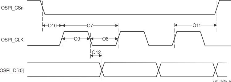
Table 6-116 defines DLL delays required for OSPI0 PHY SDR Mode. Table 6-122, Figure 6-99, Figure 6-100, Table 6-123, and Figure 6-101 present timing requirements and switching characteristics for OSPI0 PHY SDR Mode.

Table 6-116 OSPI0 DLL Delay Mapping for PHY SDR Timing Modes
MODE OSPI_PHY_CONFIGURATION_REG BIT FIELD DELAY VALUE
Transmit
All modes PHY_CONFIG_TX_DLL_DELAY_FLD, 0x0
Receive
All modes PHY_CONFIG_RX_DLL_DELAY_FLD 0x0
Table 6-117 OSPI0 Timing Requirements – PHY SDR Mode see Figure 6-99 and Figure 6-100
NO. MODE MIN MAX UNIT
O19 tsu(D-CLK) Setup time, OSPI0_D[7:0] valid before active OSPI0_CLK edge 1.8V, SDR with Internal PHY Loopback 4.8 ns
3.3V, SDR with Internal PHY Loopback 5.19 ns
O20 th(CLK-D) Hold time, OSPI0_D[7:0] valid after active OSPI0_CLK edge 1.8V, SDR with Internal PHY Loopback -0.5 ns
3.3V, SDR with Internal PHY Loopback -0.5 ns
O21 tsu(D-LBCLK) Setup time, OSPI0_D[7:0] valid before active OSPI0_DQS edge 1.8V, SDR with External Board Loopback 0.6 ns
3.3V, SDR with External Board Loopback 0.9 ns
O22 th(LBCLK-D) Hold time, OSPI0_D[7:0] valid after active OSPI0_DQS edge 1.8V, SDR with External Board Loopback 1.7 ns
3.3V, SDR with External Board Loopback 2.0 ns
TDA4VEN-Q1 TDA4AEN-Q1 OSPI0
                    Timing Requirements – PHY SDR with Internal PHY Loopback Figure 6-99 OSPI0 Timing Requirements – PHY SDR with Internal PHY Loopback
TDA4VEN-Q1 TDA4AEN-Q1 OSPI0
                    Timing Requirements – PHY SDR with External Board Loopback Figure 6-100 OSPI0 Timing Requirements – PHY SDR with External Board Loopback
Table 6-118 OSPI0 Switching Characteristics – PHY SDR Mode see Figure 6-101
NO. PARAMETER MODE MIN MAX UNIT
O7 tc(CLK) Cycle time, OSPI0_CLK 1.8V 7 ns
3.3V 6.03 ns
O8 tw(CLKL) Pulse duration, OSPI0_CLK low ((0.475P(1)) - 0.3) ns
O9 tw(CLKH) Pulse duration, OSPI0_CLK high ((0.475P(1)) - 0.3) ns
O10 td(CSn-CLK) Delay time, OSPI0_CSn[3:0] active edge to OSPI0_CLK rising edge ((0.475P(1)) + (0.975M(2)R(4)) - 1) ((0.525P(1)) + (1.025M(2)R(4)) + 1) ns
O11 td(CLK-CSn) Delay time, OSPI0_CLK rising edge to OSPI0_CSn[3:0] inactive edge ((0.475P(1)) + (0.975N(3)R(4)) - 1) ((0.525P(1)) + (1.025N(3)R(4)) + 1) ns
O12 td(CLK-D) Delay time, OSPI0_CLK active edge to OSPI0_D[7:0] transition 1.8V -1.16 1.25 ns
3.3V -1.33 1.51 ns
P = SCLK cycle time in ns = OSPI0_CLK cycle time in ns
M = OSPI_DEV_DELAY_REG[D_INIT_FLD]
N = OSPI_DEV_DELAY_REG[D_AFTER_FLD]
R = reference clock cycle time in ns
TDA4VEN-Q1 TDA4AEN-Q1 OSPI0
                    Switching Characteristics – PHY SDR Figure 6-101 OSPI0 Switching Characteristics – PHY SDR