SNAS670
July 2015
TDC1011-Q1
PRODUCTION DATA.
1
Features
2
Applications
3
Description
4
Revision History
5
Pin Configuration and Functions
6
Specifications
6.1
Absolute Maximum Ratings
6.2
ESD Ratings
6.3
Recommended Operating Conditions
6.4
Thermal Information
6.5
Electrical Characteristics
6.6
Timing Requirements
6.7
Switching Characteristics
6.8
Typical Characteristics
7
Parameter Measurement Information
8
Detailed Description
8.1
Overview
8.2
Functional Block Diagram
8.3
Feature Description
8.3.1
Transmitter Signal Path
8.3.2
Receiver Signal Path
8.3.3
Low Noise Amplifier (LNA)
8.3.4
Programmable Gain Amplifier (PGA)
8.3.5
Receiver Filters
8.3.6
Comparators for STOP Pulse Generation
8.3.6.1
Threshold Detector and DAC
8.3.6.2
Zero-cross Detect Comparator
8.3.6.3
Event Manager
8.3.7
Common-mode Buffer (VCOM)
8.3.8
Temperature Sensor
8.3.8.1
Temperature Measurement with Multiple RTDs
8.3.8.2
Temperature Measurement with a Single RTD
8.4
Device Function Description
8.4.1
Time-of-Flight Measurement Mode
8.4.1.1
Liquid Level or Fluid Identification
8.4.2
State Machine
8.4.3
TRANSMIT Operation
8.4.3.1
Transmission Pulse Count
8.4.3.2
TX 180° Pulse Shift
8.4.3.3
Transmitter Damping
8.4.4
RECEIVE Operation
8.4.4.1
Single Echo Receive Mode
8.4.4.2
Multiple Echo Receive Mode
8.4.5
Timing
8.4.5.1
Timing Control and Frequency Scaling (CLKIN)
8.4.5.2
TX/RX Measurement Sequencing and Timing
8.4.6
Time-of-Flight (TOF) Control
8.4.6.1
Short TOF Measurement
8.4.6.2
Standard TOF Measurement
8.4.6.3
Standard TOF Measurement with Power Blanking
8.4.6.4
Common-mode Reference Settling Time
8.4.6.5
TOF Measurement Interval
8.4.7
Error Reporting
8.5
Programming
8.5.1
Serial Peripheral Interface (SPI)
8.5.1.1
Chip Select Bar (CSB)
8.5.1.2
Serial Clock (SCLK)
8.5.1.3
Serial Data Input (SDI)
8.5.1.4
Serial Data Output (SDO)
8.6
Register Maps
8.6.1
TDC1011 Registers
8.6.1.1
CONFIG_0 Register (address = 0h) [reset = 45h]
8.6.1.2
CONFIG_1 Register (address = 1h) [reset = 40h]
8.6.1.3
CONFIG_2 Register (address = 2h) [reset = 0h]
8.6.1.4
CONFIG_3 Register (address 3h) [reset = 3h]
8.6.1.5
CONFIG_4 Register (address = 4h) [reset = 1Fh]
8.6.1.6
TOF_1 Register (address = 5h) [reset = 0h]
8.6.1.7
TOF_0 Register (address = 6h) [reset = 0h]
8.6.1.8
ERROR_FLAGS Register (address = 7h) [reset = 0h]
8.6.1.9
TIMEOUT Register (address = 8h) [reset = 19h]
8.6.1.10
CLOCK_RATE Register (address = 9h) [reset = 0h]
9
Application and Implementation
9.1
Application Information
9.2
Typical Applications
9.2.1
Level and Fluid Identification Measurements
9.2.1.1
Design Requirements
9.2.1.2
Detailed Design Procedure
9.2.1.2.1
Level Measurements
9.2.1.2.2
Fluid Identification
9.2.1.3
Application Curves
10
Power Supply Recommendations
11
Layout
11.1
Layout Guidelines
11.2
Layout Example
12
Device and Documentation Support
12.1
Device Support
12.1.1
Third-Party Products Disclaimer
12.1.2
Development Support
12.2
Community Resources
12.3
Trademarks
12.4
Electrostatic Discharge Caution
12.5
Glossary
13
Mechanical, Packaging, and Orderable Information
Package Options
Mechanical Data (Package|Pins)
PW|28
MPDS364
Thermal pad, mechanical data (Package|Pins)
Orderable Information
snas670_oa
snas670_pm
7 Parameter Measurement Information
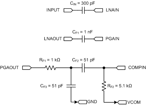
Figure 14. External Circuits for Jitter Measurement