SLLSFI6A july   2022  – july 2023 TDP1204

PRODUCTION DATA  

  1.   1
  2. Features
  3. Applications
  4. Description
  5. Revision History
  6. Pin Configuration and Functions
  7. Specifications
    1. 6.1 Absolute Maximum Ratings
    2. 6.2 ESD Ratings
    3. 6.3 Recommended Operating Conditions
    4. 6.4 Thermal Information
    5. 6.5 Electrical Characteristics
    6. 6.6 Timing Requirements
    7. 6.7 Switching Characteristics
    8. 6.8 Typical Characteristics
  8. Parameter Measurement Information
  9. Detailed Description
    1. 8.1 Functional Block Diagram
    2. 8.2 Feature Description
      1. 8.2.1  4-Level Inputs
      2. 8.2.2  I/O Voltage Level Selection
      3. 8.2.3  HPD_OUT
      4. 8.2.4  Lane Control
      5. 8.2.5  Swap
      6. 8.2.6  Linear and Limited Redriver
      7. 8.2.7  Main Link Inputs
      8. 8.2.8  Receiver Equalizer
      9. 8.2.9  CTLE Bypass
      10. 8.2.10 Adaptive Equalization in HDMI 2.1 FRL
        1. 8.2.10.1 HDMI 2.1 TX Compliance Testing with AEQ Enabled
      11. 8.2.11 HDMI 2.1 Link Training Compatible Rx EQ
      12. 8.2.12 Input Signal Detect
      13. 8.2.13 Main Link Outputs
        1. 8.2.13.1 Transmitter Bias
        2. 8.2.13.2 Transmitter Impedance Control
        3. 8.2.13.3 TX Slew Rate Control
        4. 8.2.13.4 TX Pre-Emphasis and De-Emphasis Control
        5. 8.2.13.5 TX Swing Control
      14. 8.2.14 DDC Buffer
      15. 8.2.15 HDMI DDC Capacitance
      16. 8.2.16 DisplayPort
    3. 8.3 Device Functional Modes
      1. 8.3.1 MODE Control
        1. 8.3.1.1 I2C Mode (MODE = "F")
        2. 8.3.1.2 Pin Strap Modes
          1. 8.3.1.2.1 Pin-Strap: HDMI 1.4 and HDMI 2.0 Functional Description
          2. 8.3.1.2.2 Pin-Strap HDMI 2.1 Function (MODE = "0"): Fixed Rx EQ and DDC Buffer Enabled
          3. 8.3.1.2.3 Pin-Strap HDMI 2.1 Function (MODE = "1"): Flexible RX EQ and DDC Buffer Enabled
          4. 8.3.1.2.4 Pin-Strap HDMI 2.1 Function (MODE = "R"): Flexible Rx EQ and DDC Buffer Disabled
      2. 8.3.2 DDC Snoop Feature
        1. 8.3.2.1 HDMI Type
        2. 8.3.2.2 HDMI 2.1 FRL Snoop
      3. 8.3.3 Low Power States
    4. 8.4 Programming
      1. 8.4.1 Pseudocode Examples
        1. 8.4.1.1 HDMI 2.1 Source Example with DDC Snoop and DDC Buffer Enabled
        2. 8.4.1.2 HDMI 2.1 Source Example with DDC Snoop Disabled and DDC Buffer Disabled
      2. 8.4.2 TDP1204 I2C Address Options
      3. 8.4.3 I2C Target Behavior
    5. 8.5 Register Maps
      1. 8.5.1 TDP1204 Registers
  10. Application and Implementation
    1. 9.1 Application Information
    2. 9.2 Typical Source-Side Application
      1. 9.2.1 Design Requirements
      2. 9.2.2 Detailed Design Procedure
        1. 9.2.2.1 Pre-Channel (LAB)
        2. 9.2.2.2 Post-Channel (LCD)
        3. 9.2.2.3 Common Mode Choke
        4. 9.2.2.4 ESD Protection
      3. 9.2.3 Application Curves
    3. 9.3 Typical Sink-Side Application
      1. 9.3.1 Design Requirements
      2. 9.3.2 Detailed Design Procedures
    4. 9.4 Power Supply Recommendations
      1. 9.4.1 Supply Decoupling
    5. 9.5 Layout
      1. 9.5.1 Layout Guidelines
      2. 9.5.2 Layout Example
  11. 10Device and Documentation Support
    1. 10.1 Documentation Support
      1. 10.1.1 Related Documentation
    2. 10.2 Receiving Notification of Documentation Updates
    3. 10.3 Support Resources
    4. 10.4 Trademarks
    5. 10.5 Electrostatic Discharge Caution
    6. 10.6 Glossary
  12. 11Mechanical, Packaging, and Orderable Information

Package Options

Mechanical Data (Package|Pins)
Thermal pad, mechanical data (Package|Pins)
Orderable Information

Typical Sink-Side Application

Figure 9-9 shows a schematic representation of what is considered a standard sink implementation.
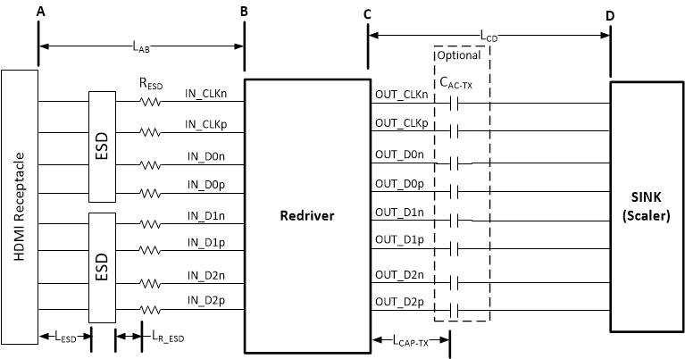
GUID-C7D02ED8-0748-497E-8E53-EBB2CDAA5DB8-low.gif Figure 9-9 TDP1204 in Sink Side Application