SLLSFI6A july 2022 – july 2023 TDP1204
PRODUCTION DATA
- 1
- 1 Features
- 2 Applications
- 3 Description
- 4 Revision History
- 5 Pin Configuration and Functions
- 6 Specifications
- 7 Parameter Measurement Information
-
8 Detailed Description
- 8.1 Functional Block Diagram
- 8.2
Feature Description
- 8.2.1 4-Level Inputs
- 8.2.2 I/O Voltage Level Selection
- 8.2.3 HPD_OUT
- 8.2.4 Lane Control
- 8.2.5 Swap
- 8.2.6 Linear and Limited Redriver
- 8.2.7 Main Link Inputs
- 8.2.8 Receiver Equalizer
- 8.2.9 CTLE Bypass
- 8.2.10 Adaptive Equalization in HDMI 2.1 FRL
- 8.2.11 HDMI 2.1 Link Training Compatible Rx EQ
- 8.2.12 Input Signal Detect
- 8.2.13 Main Link Outputs
- 8.2.14 DDC Buffer
- 8.2.15 HDMI DDC Capacitance
- 8.2.16 DisplayPort
- 8.3
Device Functional Modes
- 8.3.1
MODE Control
- 8.3.1.1 I2C Mode (MODE = "F")
- 8.3.1.2
Pin Strap Modes
- 8.3.1.2.1 Pin-Strap: HDMI 1.4 and HDMI 2.0 Functional Description
- 8.3.1.2.2 Pin-Strap HDMI 2.1 Function (MODE = "0"): Fixed Rx EQ and DDC Buffer Enabled
- 8.3.1.2.3 Pin-Strap HDMI 2.1 Function (MODE = "1"): Flexible RX EQ and DDC Buffer Enabled
- 8.3.1.2.4 Pin-Strap HDMI 2.1 Function (MODE = "R"): Flexible Rx EQ and DDC Buffer Disabled
- 8.3.2 DDC Snoop Feature
- 8.3.3 Low Power States
- 8.3.1
MODE Control
- 8.4 Programming
- 8.5 Register Maps
- 9 Application and Implementation
- 10Device and Documentation Support
- 11Mechanical, Packaging, and Orderable Information
Package Options
Mechanical Data (Package|Pins)
- RNQ|40
Thermal pad, mechanical data (Package|Pins)
Orderable Information
9.5.1 Layout Guidelines
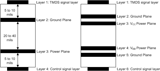
For the TDP1204 on a high-K board, it is required to solder the PowerPAD™ onto the thermal land to ground. A thermal land is the area of solder-tinned-copper underneath the PowerPAD package. On a high-K board, the TDP1204 can operate over the full temperature range by soldering the PowerPAD onto the thermal land. For the device to operate across the temperature range on a low-K board, a 1-oz Cu trace connecting the GND pins to the thermal land must be used. A simulation shows RθJA = 30.9°C/W allowing 950-mW power dissipation at 70°C ambient temperature. For information about a general PCB design guide for PowerPAD packages, refer to the PowerPAD Thermally Enhanced Package application report. TI recommends using a four layer stack up at a minimum to accomplish a low-EMI PCB design. TI recommends four layers as the TDP1204 is a single voltage rail device.
- Routing the high-speed TMDS traces on the top layer avoids the use of vias (and the introduction of their inductances) and allows for clean interconnects from the HDMI connectors to the Redriver inputs and outputs. It is important to match the electrical length of these high speed traces to minimize both inter-pair and intra-pair skew.
- Placing a solid ground plane next to the high-speed single layer establishes controlled impedance for transmission link interconnects and provides an excellent low-inductance path for the return current flow.
- Placing a power plane next to the ground plane creates an additional high-frequency bypass capacitance.
- Routing slower seed control signals on the bottom layer allows for greater flexibility as these signal links usually have margin to tolerate discontinuities such as vias.
- If an additional supply voltage plane or signal layer is needed, add a second power or ground plane system to the stack to keep symmetry. This makes the stack mechanically stable and prevents it from warping. Also the power and ground plane of each power system can be placed closer together, thus increasing the high frequency bypass capacitance significantly.
- To minimize crosstalk between adjacent differential pairs, the distance between the differential pairs should be at least five times longer than the trace width (5W rule). For the clock differential pair, the distance should be increased to 8W or 10W.
 Figure 9-11 Recommended 4 or 6-Layer PCB Stack