SLLSG10 November 2024 TDP142-Q1
ADVANCE INFORMATION
- 1
- 1 Features
- 2 Applications
- 3 Description
- 4 Pin Configuration and Functions
- 5 Specifications
- Parameter Measurement Information
- 6 Detailed Description
- 7 Register Maps
- 8 Application and Implementation
- 9 Device and Documentation Support
- 10Revision History
- 11Mechanical, Packaging, and Orderable Information
Package Options
Mechanical Data (Package|Pins)
- RGF|40
Thermal pad, mechanical data (Package|Pins)
Orderable Information
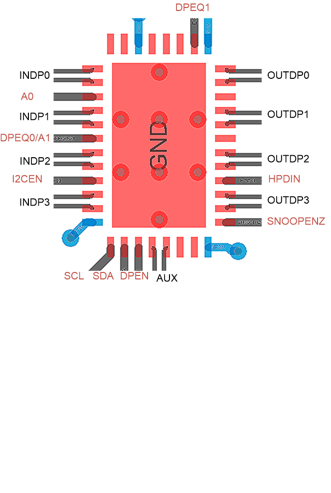
8.4.2 Layout Example
 Figure 8-6 Layout Example
The following figures demonstrate the solution of mismatched order between the output of the device and the DisplayPort connector for the source using BGA package. Figure 8-7 shows the crossing section between TDP142-Q1 and connector. Usually, vias are applied to avoid the cross, but using a via can attenuate the signal integrity. Therefore, the polarity swap can be implemented at the input of TDP142-Q1. Figure 8-8 shows there is no more crossing section between the TDP142-Q1 and connector, which can minimize the number of vias being used. Note that the solution is only useful for the source using BGA package.

Figure 8-7 Layout Example: Signal Crossing on the Output

Figure 8-8 Layout Example: INDP2 and INDP3 Polarity Swap