SLLSG10 November   2024 TDP142-Q1

ADVANCE INFORMATION  

  1.   1
  2. Features
  3. Applications
  4. Description
  5. Pin Configuration and Functions
  6. Specifications
    1. 5.1 Absolute Maximum Ratings
    2. 5.2 ESD Ratings
    3. 5.3 Recommended Operating Conditions
    4. 5.4 Thermal Information
    5. 5.5 Power Supply Characteristics
    6. 5.6 Control I/O DC Electrical Characteristics
    7. 5.7 DP Electrical Characteristics
    8. 5.8 Switching Characteristics
    9. 5.9 Typical Characteristics
  7.   Parameter Measurement Information
  8. Detailed Description
    1. 6.1 Overview
    2. 6.2 Functional Block Diagram
    3. 6.3 Feature Description
      1. 6.3.1 DisplayPort
      2. 6.3.2 Configuration Jumper Levels
      3. 6.3.3 Receiver Linear Equalization
    4. 6.4 Device Functional Modes
      1. 6.4.1 Device Configuration in GPIO Mode
      2. 6.4.2 Device Configuration in I2C Mode
      3. 6.4.3 Linear EQ Configuration
      4. 6.4.4 Operation Timing – Power Up
    5. 6.5 Programming
  9. Register Maps
    1. 7.1 TDP142-Q1 Registers
  10. Application and Implementation
    1. 8.1 Application Information
      1. 8.1.1 ESD Protection
    2. 8.2 Typical Application
      1. 8.2.1 Source Application Implementation
        1. 8.2.1.1 Design Requirement
        2. 8.2.1.2 Detail Design Procedure
      2. 8.2.2 Sink Application Implementation
        1. 8.2.2.1 Design Requirements
        2. 8.2.2.2 Detailed Design Procedure
      3. 8.2.3 Application Curve
    3. 8.3 Power Supply Recommendations
    4. 8.4 Layout
      1. 8.4.1 Layout Guidelines
      2. 8.4.2 Layout Example
  11. Device and Documentation Support
    1. 9.1 Receiving Notification of Documentation Updates
    2. 9.2 Support Resources
    3. 9.3 Trademarks
    4. 9.4 Electrostatic Discharge Caution
    5. 9.5 Glossary
  12. 10Revision History
  13. 11Mechanical, Packaging, and Orderable Information
    1. 11.1 Tape and Reel Information
    2. 11.2 Mechanical Data

Package Options

Mechanical Data (Package|Pins)
Thermal pad, mechanical data (Package|Pins)
Orderable Information

Application Information

The TDP142-Q1 is a linear redriver designed specifically to compensate the inter-symbol interference (ISI) jitter caused by signal attenuation through a passive medium like PCB traces and cable. The device can be used in source, sink, and cable applications, where the device is transparent to the link training. For illustrating purposes, this section shows the implementations of source application and sink application. Figure 8-1 and Figure 8-2 are the high level block diagram for DisplayPort source side application and DisplayPort sink side application respectively, where the TDP142-Q1 is snooping both channels of AUX signal and HPD signal.
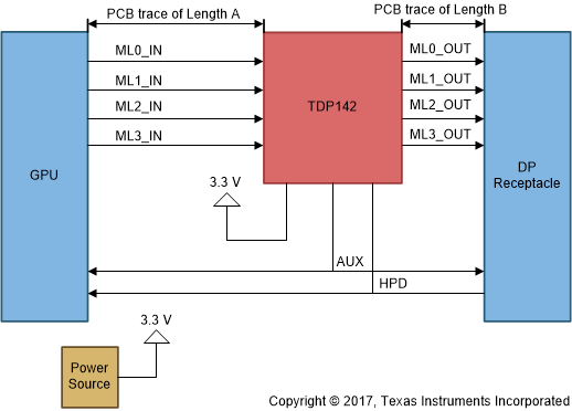
TDP142-Q1 Source Application for TDP142-Q1Figure 8-1 Source Application for TDP142-Q1
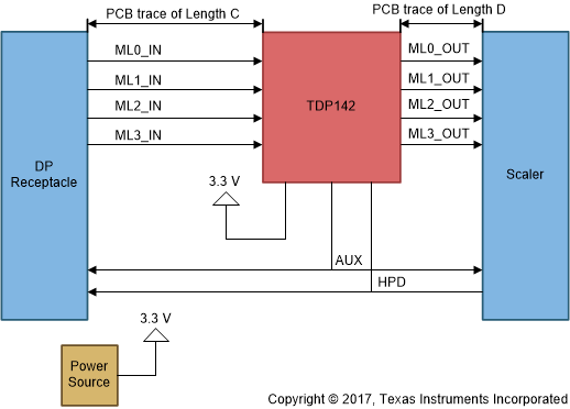
TDP142-Q1 Sink Application for TDP142-Q1Figure 8-2 Sink Application for TDP142-Q1