SLLSG10 November   2024 TDP142-Q1

ADVANCE INFORMATION  

  1.   1
  2. Features
  3. Applications
  4. Description
  5. Pin Configuration and Functions
  6. Specifications
    1. 5.1 Absolute Maximum Ratings
    2. 5.2 ESD Ratings
    3. 5.3 Recommended Operating Conditions
    4. 5.4 Thermal Information
    5. 5.5 Power Supply Characteristics
    6. 5.6 Control I/O DC Electrical Characteristics
    7. 5.7 DP Electrical Characteristics
    8. 5.8 Switching Characteristics
    9. 5.9 Typical Characteristics
  7.   Parameter Measurement Information
  8. Detailed Description
    1. 6.1 Overview
    2. 6.2 Functional Block Diagram
    3. 6.3 Feature Description
      1. 6.3.1 DisplayPort
      2. 6.3.2 Configuration Jumper Levels
      3. 6.3.3 Receiver Linear Equalization
    4. 6.4 Device Functional Modes
      1. 6.4.1 Device Configuration in GPIO Mode
      2. 6.4.2 Device Configuration in I2C Mode
      3. 6.4.3 Linear EQ Configuration
      4. 6.4.4 Operation Timing – Power Up
    5. 6.5 Programming
  9. Register Maps
    1. 7.1 TDP142-Q1 Registers
  10. Application and Implementation
    1. 8.1 Application Information
      1. 8.1.1 ESD Protection
    2. 8.2 Typical Application
      1. 8.2.1 Source Application Implementation
        1. 8.2.1.1 Design Requirement
        2. 8.2.1.2 Detail Design Procedure
      2. 8.2.2 Sink Application Implementation
        1. 8.2.2.1 Design Requirements
        2. 8.2.2.2 Detailed Design Procedure
      3. 8.2.3 Application Curve
    3. 8.3 Power Supply Recommendations
    4. 8.4 Layout
      1. 8.4.1 Layout Guidelines
      2. 8.4.2 Layout Example
  11. Device and Documentation Support
    1. 9.1 Receiving Notification of Documentation Updates
    2. 9.2 Support Resources
    3. 9.3 Trademarks
    4. 9.4 Electrostatic Discharge Caution
    5. 9.5 Glossary
  12. 10Revision History
  13. 11Mechanical, Packaging, and Orderable Information
    1. 11.1 Tape and Reel Information
    2. 11.2 Mechanical Data

Package Options

Mechanical Data (Package|Pins)
Thermal pad, mechanical data (Package|Pins)
Orderable Information

Description

The TDP142-Q1 is a DisplayPort™ (DP) linear redriver that is able to snoop AUX and HPD signals. The device complies with the VESA® DisplayPort™ standard Version 1.4, and supports a 1-lane to 4-lane Main Link interface signaling up to HBR3 (8.1Gbps per lane). Additionally, this device is position independent. The TDP142-Q1 can be placed inside source, cable or sink effectively providing a "negative loss" component to the overall link budget.

The TDP142-Q1 provides several levels of receive linear equalization to compensate for cable and board trace loss due to inter symbol interference (ISI). The TDP142-Q1 operates on a single 3.3V supply and comes in an automotive grade 2 temperature range.
Package Information
PART NUMBERPACKAGE(1)PACKAGE SIZE(2)
TDP142-Q1RGF (VQFN, 40)7mm × 5mm
For all available packages, see the orderable addendum at the end of the data sheet.
The package size (length × width) is a nominal value and includes pins, where applicable.
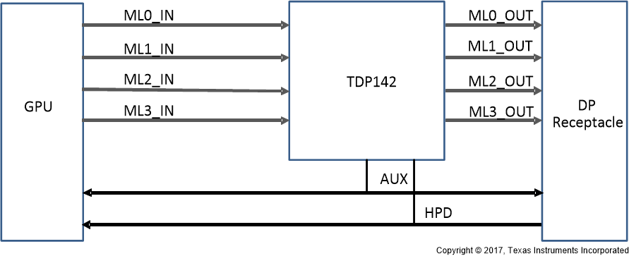
TDP142-Q1 Simplified SchematicSimplified Schematic
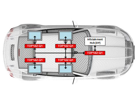
TDP142-Q1 Application Use CaseApplication Use Case