SLDS190B November 2012 – March 2022 TFP401A-Q1
PRODUCTION DATA
- 1 Features
- 2 Applications
- 3 Description
- 4 Revision History
- 5 Pin Configuration and Functions
-
6 Specifications
- 6.1 Absolute Maximum Ratings
- 6.2 ESD Ratings
- 6.3 Recommended Operating Conditions
- 6.4 Thermal Information
- 6.5 DC Digital I/O Electrical Characteristics
- 6.6 DC Electrical Characteristics
- 6.7 AC Electrical Characteristics
- 6.8 Timing Requirements
- 6.9 Switching Characteristics
- 6.10 Typical Characteristics
- 7 Detailed Description
- 8 Application and Implementation
- 9 Device and Documentation Support
- 10Mechanical, Packaging, and Orderable Information
Package Options
Mechanical Data (Package|Pins)
- PZP|100
Thermal pad, mechanical data (Package|Pins)
- PZP|100
Orderable Information
6.9 Switching Characteristics
over operating free-air temperature range (unless otherwise noted)
| PARAMETER | TEST CONDITIONS | MIN | TYP | MAX | UNIT | |
|---|---|---|---|---|---|---|
| tpd(PDL) | Propagation delay time from PD low to Hi-Z outputs | 9 | ns | |||
| tpd(PDOL) | Propagation delay time from PDO low to Hi-Z outputs | 9 | ns | |||
| tt(HSC) | Delay time from DE transition to SCDT low(7) | 1e6 | tpix | |||
| tt(FSC) | Delay time from DE transition to SCDT high(7) | 1600 | tpix | |||
| td(st) | Delay time, ODCK latching edge to QE[23:0] data output | STAG = low, PIXS = high | 0.25 | tpix | ||
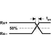
 Figure 6-10 Analog Input Intra-Pair Differential Skew
 Figure 6-11 Minimum Time
PD Low
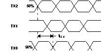
 Figure 6-12 Analog Input Channel-to-Channel Skew
 Figure 6-13 Minimum DE Low and Maximum DE High