SLDS190B November 2012 – March 2022 TFP401A-Q1
PRODUCTION DATA
- 1 Features
- 2 Applications
- 3 Description
- 4 Revision History
- 5 Pin Configuration and Functions
-
6 Specifications
- 6.1 Absolute Maximum Ratings
- 6.2 ESD Ratings
- 6.3 Recommended Operating Conditions
- 6.4 Thermal Information
- 6.5 DC Digital I/O Electrical Characteristics
- 6.6 DC Electrical Characteristics
- 6.7 AC Electrical Characteristics
- 6.8 Timing Requirements
- 6.9 Switching Characteristics
- 6.10 Typical Characteristics
- 7 Detailed Description
- 8 Application and Implementation
- 9 Device and Documentation Support
- 10Mechanical, Packaging, and Orderable Information
Package Options
Mechanical Data (Package|Pins)
- PZP|100
Thermal pad, mechanical data (Package|Pins)
- PZP|100
Orderable Information
3 Description
The Texas Instruments TFP401A-Q1 device is a TI Panelbus™ flat-panel display product, and is part of a comprehensive family of end-to-end DVI 1.0-compliant solutions. Targeted primarily at desktop LCD monitors and digital projectors, the TFP401A-Q1 device finds applications in any design requiring high-speed digital interface.
The TFP401A-Q1 device supports display resolutions up to 1080p and WUXGA in 24-bit true-color pixel format. It also offers design flexibility to drive one or two pixels per clock, supports TFT or DSTN panels, and provides an option for time-staggered pixel outputs for reduced ground bounce.
PowerPAD advanced packaging technology results in best-of-class power dissipation, footprint, and ultralow ground inductance.
The TFP401A-Q1 combines Panelbus circuit innovation with TI's advanced 0.18-µm EPIC-5™ CMOS process technology, along with TI PowerPAD package technology to achieve a reliable, low-powered, low-noise, high-speed digital interface solution.
| PART NUMBER | PACKAGE | BODY SIZE (NOM) |
|---|---|---|
| TFP401A-Q1 | PQFP (100) | 14.00 mm × 14.00 mm |
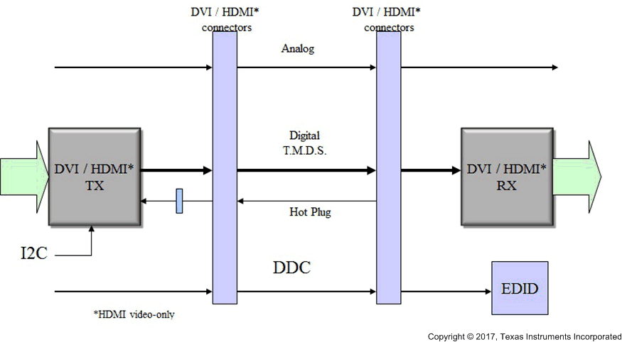
 TFP401A-Q1 Diagram