SLOS382E September 2001 – May 2015 THS3122 , THS3125
PRODUCTION DATA.
- 1 Features
- 2 Applications
- 3 Description
- 4 Revision History
- 5 Device Options
- 6 Pin Configuration and Functions
-
7 Specifications
- 7.1 Absolute Maximum Ratings
- 7.2 Dissipation Ratings Table
- 7.3 Recommended Operating Conditions
- 7.4 Electrical Characteristics: Dynamic Performance
- 7.5 Electrical Characteristics: Noise and Distortion Performance
- 7.6 Electrical Characteristics: DC Performance
- 7.7 Electrical Characteristics: Input Characteristics
- 7.8 Electrical Characteristics: Output Characteristics
- 7.9 Electrical Characteristics: Power Supply
- 7.10 Electrical Characteristics: Shutdown Characteristics (THS3125 Only)
- 7.11 Typical Characteristics: Table Of Graphs
- 7.12 Typical Characteristics
- 8 Detailed Description
- 9 Application and Implementation
- 10Layout
- 11Device and Documentation Support
- 12Mechanical, Packaging, and Orderable Information
Package Options
Mechanical Data (Package|Pins)
Thermal pad, mechanical data (Package|Pins)
- DDA|8
Orderable Information
9 Application and Implementation
NOTE
Information in the following applications sections is not part of the TI component specification, and TI does not warrant its accuracy or completeness. TI’s customers are responsible for determining suitability of components for their purposes. Customers should validate and test their design implementation to confirm system functionality.
9.1 Application Information
9.1.1 Video Distribution
The wide bandwidth, high slew rate, and high output drive current of the THS3125 and THS3122 match the demands for video distribution to deliver video signals down multiple cables. To ensure high signal quality with minimal degradation of performance, a 0.1-dB gain flatness should be at least 7x the passband frequency to minimize group delay variations from the amplifier. A high slew rate minimizes distortion of the video signal, and supports component video and RGB video signals that require fast transition times and fast settling times for high signal quality. Figure 40 illustrates a typical video distribution amplifier application configuration.
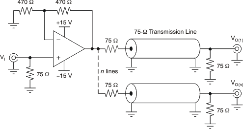 Figure 40. Video Distribution Amplifier Application
9.1.2 Driving Capacitive Loads
Applications such as FET drivers and line drivers can be highly capacitive and cause stability problems for high-speed amplifiers.
Figure 41 through Figure 47 show recommended methods for driving capacitive loads. The basic idea is to use a resistor or ferrite chip to isolate the phase shift at high frequency caused by the capacitive load from the amplifier feedback path. See Figure 41 for recommended resistor values versus capacitive load.
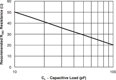 Figure 41. Recommended RISO vs Capacitive Load
Placing a small series resistor, RISO, between the amplifier output and the capacitive load, as shown in Figure 42, is an easy way of isolating the load capacitance.
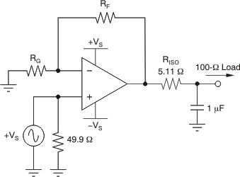 Figure 42. Resistor To Isolate Capacitive Load
Using a ferrite chip in place of RISO, as Figure 43 shows, is another approach of isolating the output of the amplifier. The ferrite impedance characteristic versus frequency is useful to maintain the low frequency load independence of the amplifier while isolating the phase shift caused by the capacitance at high frequency. Use a ferrite with similar impedance to RISO, 20 Ω to 50 Ω, at 100 MHz and low impedance at dc.
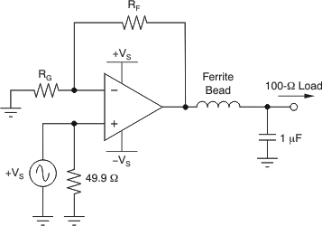 Figure 43. Ferrite Bead To Isolate Capacitive Load
Figure 44 shows another method used to maintain the low-frequency load independence of the amplifier while isolating the phase shift caused by the capacitance at high frequency. At low frequency, feedback is mainly from the load side of RISO. At high frequency, the feedback is mainly via the 27-pF capacitor. The resistor RIN in series with the negative input is used to stabilize the amplifier and should be equal to the recommended value of RF at unity gain. Replacing RIN with a ferrite of similar impedance at about 100 MHz as shown in Figure 45 gives similar results with reduced dc offset and low frequency noise.
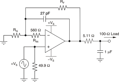 Figure 44. Feedback Technique With Input Resistor For Capacitive Load
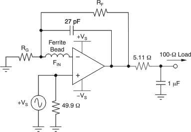 Figure 45. Feedback Technique With Input Ferrite Bead For Capacitive Load
Figure 46 shows a configuration that uses two amplifiers in parallel to double the output drive current to larger capacitive loads. This technique is used when more output current is needed to charge and discharge the load faster as when driving large FET transistors.
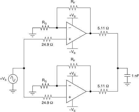 Figure 46. Parallel Amplifiers For Higher Output Drive
Figure 47 shows a push-pull FET driver circuit typical of ultrasound applications with isolation resistors to isolate the gate capacitance from the amplifier.
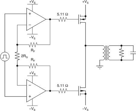 Figure 47. Powerfet Drive Circuit