SBOS780C March 2016 – June 2021 THS3215
PRODUCTION DATA
- 1 Features
- 2 Applications
- 3 Description
- 4 Revision History
- 5 Pin Configuration and Functions
-
6 Specifications
- 6.1 Absolute Maximum Ratings
- 6.2 ESD Ratings
- 6.3 Recommended Operating Conditions
- 6.4 Thermal Information
- 6.5 Electrical Characteristics: D2S
- 6.6 Electrical Characteristics: OPS
- 6.7 Electrical Characteristics: D2S + OPS
- 6.8 Electrical Characteristics: Midscale (DC) Reference Buffer
- 6.9 Typical Characteristics: D2S + OPS
- 6.10 Typical Characteristics: D2S Only
- 6.11 Typical Characteristics: OPS Only
- 6.12 Typical Characteristics: Midscale (DC) Reference Buffer
- 6.13 Typical Characteristics: Switching Performance
- 6.14 Typical Characteristics: Gain Drift
- 7 Parameter Measurement Information
-
8 Detailed Description
- 8.1 Overview
- 8.2 Functional Block Diagram
- 8.3 Feature Description
- 8.4 Device Functional Modes
-
9 Application and Implementation
- 9.1
Application Information
- 9.1.1
Typical Applications
- 9.1.1.1 High-Frequency, High-Voltage, Dual-Output Line Driver for AWGs
- 9.1.1.2 High-Voltage Pulse-Generator
- 9.1.1.3 Single-Supply, AC-Coupled, Piezo Element Driver
- 9.1.1.4 Output Common-Mode Control Using the Midscale Buffer as a Level Shifter
- 9.1.1.5 Differential I/O Driver With independent Common-Mode Control
- 9.1.1
Typical Applications
- 9.1
Application Information
- 10Power Supply Recommendations
- 11Layout
- 12Device and Documentation Support
- 13Mechanical, Packaging, and Orderable Information
Package Options
Mechanical Data (Package|Pins)
- RGV|16
Thermal pad, mechanical data (Package|Pins)
Orderable Information
6.14 Typical Characteristics: Gain Drift
at +VCC = 6 V, –VCC = –6 V, 50-Ω D2S source impedance , VIC = 0.25 V, internal path selected (PATHSEL = GND), VREF = GND, D2S RLOAD = 100 Ω at pin 6, RF = 249 Ω, RG = 162 Ω, OPS on (DISABLE = GND), OPS RLOAD = 100 Ω at pin 11, and TJ ≈ 25°C (unless otherwise noted)
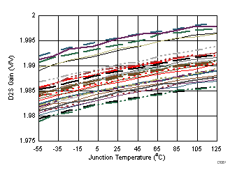
| 30 units shown |
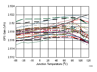
| 30 units shown |
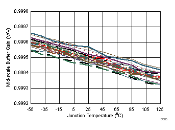
| 30 units shown | ||
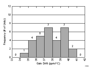
| 30 units from –40°C to +125°C |
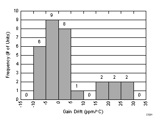
| 30 units from –40°C to +125°C |
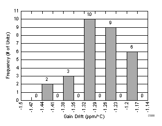
| 30 units from –40°C to +125°C |