SBOS780C March 2016 – June 2021 THS3215
PRODUCTION DATA
- 1 Features
- 2 Applications
- 3 Description
- 4 Revision History
- 5 Pin Configuration and Functions
-
6 Specifications
- 6.1 Absolute Maximum Ratings
- 6.2 ESD Ratings
- 6.3 Recommended Operating Conditions
- 6.4 Thermal Information
- 6.5 Electrical Characteristics: D2S
- 6.6 Electrical Characteristics: OPS
- 6.7 Electrical Characteristics: D2S + OPS
- 6.8 Electrical Characteristics: Midscale (DC) Reference Buffer
- 6.9 Typical Characteristics: D2S + OPS
- 6.10 Typical Characteristics: D2S Only
- 6.11 Typical Characteristics: OPS Only
- 6.12 Typical Characteristics: Midscale (DC) Reference Buffer
- 6.13 Typical Characteristics: Switching Performance
- 6.14 Typical Characteristics: Gain Drift
- 7 Parameter Measurement Information
-
8 Detailed Description
- 8.1 Overview
- 8.2 Functional Block Diagram
- 8.3 Feature Description
- 8.4 Device Functional Modes
-
9 Application and Implementation
- 9.1
Application Information
- 9.1.1
Typical Applications
- 9.1.1.1 High-Frequency, High-Voltage, Dual-Output Line Driver for AWGs
- 9.1.1.2 High-Voltage Pulse-Generator
- 9.1.1.3 Single-Supply, AC-Coupled, Piezo Element Driver
- 9.1.1.4 Output Common-Mode Control Using the Midscale Buffer as a Level Shifter
- 9.1.1.5 Differential I/O Driver With independent Common-Mode Control
- 9.1.1
Typical Applications
- 9.1
Application Information
- 10Power Supply Recommendations
- 11Layout
- 12Device and Documentation Support
- 13Mechanical, Packaging, and Orderable Information
Package Options
Mechanical Data (Package|Pins)
- RGV|16
Thermal pad, mechanical data (Package|Pins)
- RGV|16
Orderable Information
8.3.3.1 Output DC Offset and Drift for the OPS
The OPS provides modest dc precision with typical, minimum, and maximum dc error terms in Table 8-4. The input offset voltage applies to either input path with very little difference between the internal and external paths.
| PARAMETER | TYPICAL | MINIMUM | MAXIMUM | UNIT |
|---|---|---|---|---|
| VIO | ±1 | –15 | 15 | mV |
| Ibn | 5 | –5 | 15 | µA |
| Ibi | ±5 | –75 | 75 | µA |
Selecting the internal path results in no source resistance for Ibn, so that term drops out. When the external path is selected, a dc source impedance may be present, so the Ibn term creates another error term, and adds to the total output offset.
Stepping through an example design for the OPS output dc offset using the external path with a low insertion loss filter shown in Figure 8-17, along with its RF and RG values, gives the following results:
- RS for the Ibn term = 90.9 Ω || 464 Ω = 76 Ω. (dc source impedance for the filter design)
- RF including the internal 18.5 kΩ resistor = 205 Ω || 18.5 kΩ = 202.7 Ω
- Resulting gain with the 102 Ω RG element = 2.99 V/V
Table 8-5 shows the typical and worst-case output error terms. Note that a positive current out of the noninverting input gives a positive output offset term, whereas a positive current out of the inverting input gives a negative output term.
| ERROR TERM | TYPICAL | MINIMUM | MAXIMUM | UNIT |
|---|---|---|---|---|
| Ibn × RS × AV | 1.136 | –1.136 | 3.408 | mV |
| VIO × AV | ±2.99 | –44.85 | 44.85 | mV |
| Ibi × RF | ±1.014 | –15.203 | 15.203 | mV |
| Total error | –2.87 to +5.14 | –61.19 | 63.46 | mV |
The input offset voltage dominates the error terms. The worst-case numbers are calculated by adding the individual errors algebraically, but is rarely seen in practice. None of the OPS input dc error terms are correlated. To compute output drift numbers, use the same gains shown in Table 8-5 with the specified drift numbers.
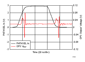
The OPS PATHSEL control responds extremely quickly with low-switching glitches, as shown in Figure 8-11. For this test, the D2S input is set to GND, and the output of the D2S is connected to the external OPS input. The PATHSEL switch is then toggled at 10 MHz. The results show the offset between the internal and external paths as well matched.
 Figure 8-11 OPS
Path-Select Switching Glitch
Figure 8-11 OPS
Path-Select Switching GlitchThe OPS includes a disable feature that reduces power consumption from approximately 11 mA to 2 mA. The logic controls are intended to be ground-referenced regardless of the power supplies used. The logic reference (GND, pin 7) is normally grounded and also provides a connection to the internal 18.5 kΩ resistor on VIN+ (pin 9, default bias to pin 7). Operating in a single-supply configuration with –VCC at GND and the external OPS input (VIN+) floated, places VIN+ internally at –VCC = GND. Driving the external OPS input (VIN+) from a source within the operating range overrides the bias to –VCC. However, if the application requires VIN+ to be floated in a single-supply operation, consider centering the voltage on VIN+ with an added 18.5 kΩ external resistor to the +VCC supply.
If the disable feature is not needed, simply float or ground DISABLE (pin 10) to hold the OPS in the enabled state. Increasing the voltage on the DISABLE pin to greater than 1.3 V disables the OPS and reduces the current to approximately 2 mA. In a single-supply design, the OPS can be disabled by setting DISABLE to +VCC, even up to the maximum operating supply of 15.8 V.
Do not move the logic threshold away from those set by the logic ground at pin 7. If a different logic swing level is required, and GND (pin 7) is biased to a different voltage, be sure the source can sink the typical 280 µA coming out of GND. Also recognize that the 18.5 kΩ bias resistor on the external OPS input (VIN+) is connected to GND voltage internally.
As shown in Figure 6-56, the OPS enables in approximately 100 ns from the logic threshold at 1.0 V, while disabling to a final value in approximately 500 ns.