SBOS780C March   2016  – June 2021 THS3215

PRODUCTION DATA  

  1. Features
  2. Applications
  3. Description
  4. Revision History
  5. Pin Configuration and Functions
  6. Specifications
    1. 6.1  Absolute Maximum Ratings
    2. 6.2  ESD Ratings
    3. 6.3  Recommended Operating Conditions
    4. 6.4  Thermal Information
    5. 6.5  Electrical Characteristics: D2S
    6. 6.6  Electrical Characteristics: OPS
    7. 6.7  Electrical Characteristics: D2S + OPS
    8. 6.8  Electrical Characteristics: Midscale (DC) Reference Buffer
    9. 6.9  Typical Characteristics: D2S + OPS
    10. 6.10 Typical Characteristics: D2S Only
    11. 6.11 Typical Characteristics: OPS Only
    12. 6.12 Typical Characteristics: Midscale (DC) Reference Buffer
    13. 6.13 Typical Characteristics: Switching Performance
    14. 6.14 Typical Characteristics: Gain Drift
  7. Parameter Measurement Information
    1. 7.1 Overview
    2. 7.2 Frequency Response Measurement
    3. 7.3 Harmonic Distortion Measurement
    4. 7.4 Noise Measurement
    5. 7.5 Output Impedance Measurement
    6. 7.6 Step-Response Measurement
    7. 7.7 Feedthrough Measurement
    8. 7.8 Midscale Buffer ROUT Versus CLOAD Measurement
  8. Detailed Description
    1. 8.1 Overview
    2. 8.2 Functional Block Diagram
    3. 8.3 Feature Description
      1. 8.3.1 Differential to Single-Ended Stage (D2S) With Fixed Gain of 2 V/V (Pins 2, 3, 6, and 14)
      2. 8.3.2 Midscale (DC) Reference Buffer (Pin 1 and Pin 15)
      3. 8.3.3 Output Power Stage (OPS) (Pins 4, 7, 9, 10, 11, and 12)
        1. 8.3.3.1 Output DC Offset and Drift for the OPS
        2. 8.3.3.2 OPS Harmonic Distortion (HD) Performance
        3. 8.3.3.3 Switch Feedthrough to the OPS
        4. 8.3.3.4 Driving Capacitive Loads
      4. 8.3.4 Digital Control Lines
    4. 8.4 Device Functional Modes
      1. 8.4.1 Full-Signal Path Mode
        1. 8.4.1.1 Internal Connection With Fixed Common-Mode Output Voltage
        2. 8.4.1.2 Internal Connection With Adjustable Common-Mode Output Voltage
        3. 8.4.1.3 External Connection
      2. 8.4.2 Dual-Output Mode
      3. 8.4.3 Differential I/O Voltage Mode
  9. Application and Implementation
    1. 9.1 Application Information
      1. 9.1.1 Typical Applications
        1. 9.1.1.1 High-Frequency, High-Voltage, Dual-Output Line Driver for AWGs
          1. 9.1.1.1.1 Design Requirements
          2. 9.1.1.1.2 Detailed Design Procedure
          3. 9.1.1.1.3 Application Curves
        2. 9.1.1.2 High-Voltage Pulse-Generator
          1. 9.1.1.2.1 Design Requirements
          2. 9.1.1.2.2 Detailed Design Procedure
          3. 9.1.1.2.3 Application Curves
        3. 9.1.1.3 Single-Supply, AC-Coupled, Piezo Element Driver
          1. 9.1.1.3.1 Detailed Design Procedure
        4. 9.1.1.4 Output Common-Mode Control Using the Midscale Buffer as a Level Shifter
          1. 9.1.1.4.1 Detailed Design Procedure
        5. 9.1.1.5 Differential I/O Driver With independent Common-Mode Control
          1. 9.1.1.5.1 Detailed Design Procedure
  10. 10Power Supply Recommendations
    1. 10.1 Thermal Considerations
  11. 11Layout
    1. 11.1 Layout Guidelines
    2. 11.2 Layout Example
  12. 12Device and Documentation Support
    1. 12.1 Device Support
      1. 12.1.1 Development Support
        1. 12.1.1.1 TINA-TI (Free Software Download)
    2. 12.2 Documentation Support
      1. 12.2.1 Related Documentation
    3. 12.3 Receiving Notification of Documentation Updates
    4. 12.4 Support Resources
    5. 12.5 Trademarks
    6. 12.6 Electrostatic Discharge Caution
    7. 12.7 Glossary
  13. 13Mechanical, Packaging, and Orderable Information

Package Options

Mechanical Data (Package|Pins)
Thermal pad, mechanical data (Package|Pins)
Orderable Information

Typical Characteristics: OPS Only

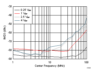
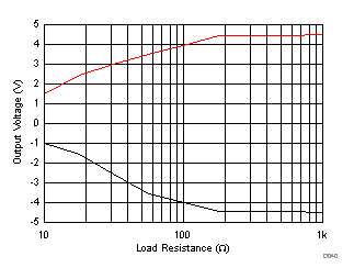
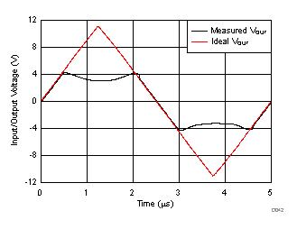
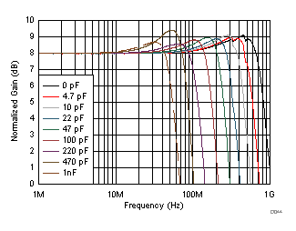
at +VCC = 6.0 V, –VCC = –6.0 V, 25-Ω D2S source impedance, VREF = GND, RF = 249 Ω, RG = 162 Ω, OPS AV = 2.5V/V, OPS RLOAD = 100 Ω at pin 11, OPS enabled (DISABLE = GND), external input path selected (PATHSEL = +VCC), and TJ ≈ 25°C (unless otherwise noted)
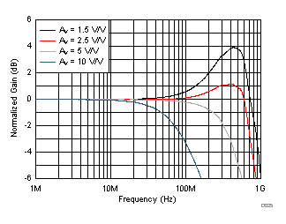
GUID-25D3E136-B546-4AE8-BC48-0C6F6835F90B-low.gif
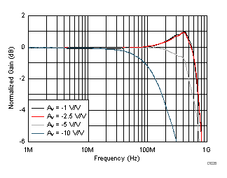
VOUT = 100 mVPP, see Table 8-1 for RF values vs gain
Figure 6-25 Frequency Response vs Noninverting Gain
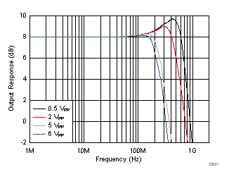
GUID-DE2BEA3F-806E-4552-B765-12662FF9E198-low.gifFigure 6-27 Noninverting Response vs Output Voltage
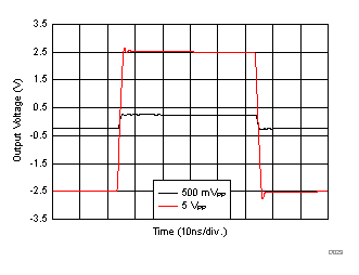
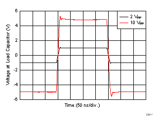
GUID-51A1DC63-50F6-46AD-A533-EE45F0506785-low.gifFigure 6-29 Noninverting Step Response
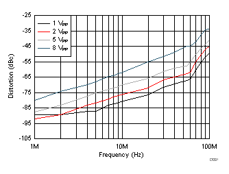
GUID-F2597524-FCCF-48A9-9EEF-8D06D9686500-low.gifFigure 6-31 HD2 vs Output Voltage
GUID-FB3E2877-49D1-4C52-B93D-B6EFAFA79ECD-low.gif
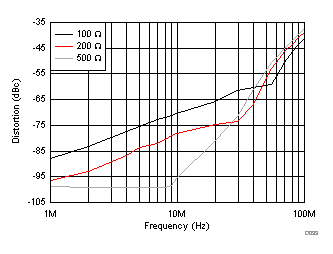
VOUT = 5 VPP
Figure 6-33 HD2 vs Load Resistance
GUID-7703C86C-7114-47BE-8DC8-47267FBE668E-low.gif
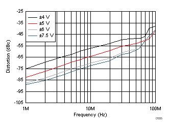
VOUT = 5 VPP
Figure 6-35 HD2 vs Supply Voltage
GUID-E7E3104B-3443-4128-8E76-3430D1992D29-low.gif
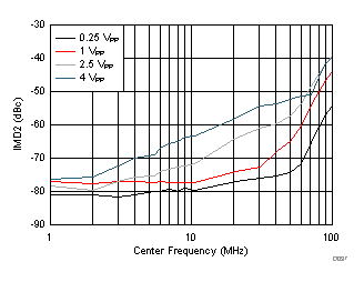
±100-kHz tone separation, output voltage for each tone
Figure 6-37 Second-Order Intermodulation Distortion vs Output Voltage
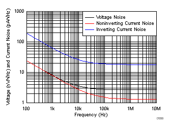
GUID-479D7651-3602-493F-89C8-BC5966EDF00C-low.gifFigure 6-39 Input-Referred Spot Noise vs Frequency
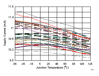
GUID-F265EE6A-5B2B-48D0-8B8A-CA370E8A00AD-low.gif
30 units shown
Figure 6-41 Quiescent Supply Current vs Temperature
GUID-487F94F8-75AC-4133-9BA5-F78C978F0A9F-low.gif
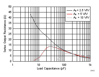
See Table 8-6 for RF values vs OPS gain
Figure 6-43 Series Output Resistance vs Load Capacitance
GUID-6793C4B3-00D5-4872-85FD-BFBD332A21A2-low.gif
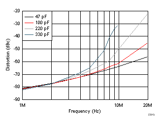
±VCC = ±7.5 V, RF = 158 Ω, AV = 5 V/V, VOUT = 10 VPP, see Figure 6-43 for RS value
Figure 6-45 HD2 vs Load Capacitance
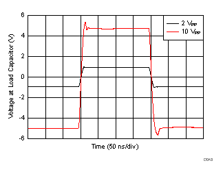
GUID-5902D563-7879-4810-BC97-D15D00C5CAC0-low.gif
±VCC = ±7.5 V, CLOAD = 100 pF, RF = 158 Ω, AV = 5 V/V, see Figure 6-43 for RS value
Figure 6-47 Pulse Response
GUID-9B28612C-028A-41C5-95A6-D952CD43A430-low.gif
VOUT = 100 mVPP, see Table 8-3 for RF values vs gain
Figure 6-26 Frequency Response vs Inverting Gain
GUID-2E84343D-CA9D-4BDD-9E38-915E973FCDF6-low.gif
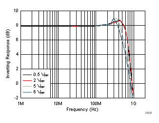
AV = –2.5 V/V, see Table 8-3 for RF value
Figure 6-28 Inverting Response vs Output Voltage
GUID-600BD99C-7F59-459C-A1C0-BD6537D6F69D-low.gif
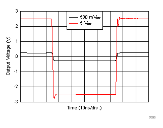
AV = –2.5 V/V, see Table 8-3 for RF value
Figure 6-30 Inverting Step Response
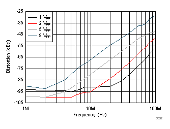
GUID-3AF02026-7E28-4637-817A-97C9463C0F9D-low.gifFigure 6-32 HD3 vs Output Voltage
GUID-E06EA654-331B-4AA2-AADA-DE5FA66FA804-low.gif
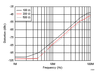
VOUT = 5 VPP
Figure 6-34 HD3 vs Load Resistance
GUID-EAB64467-F2A0-44BF-89AC-120C83045516-low.gif
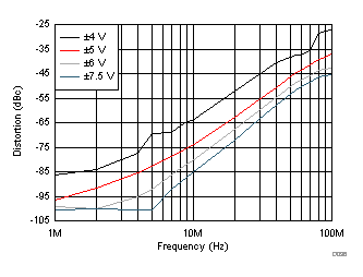
VOUT = 5 VPP
Figure 6-36 HD3 vs Supply Voltage
GUID-2D628040-6BE0-4999-B894-AAD357C3B5BC-low.gif
±100-kHz tone separation, output voltage for each tone
Figure 6-38 Third-Order Intermodulation Distortion vs Output Voltage
GUID-600B485D-95DE-4B81-A68E-0DB777E68538-low.gif
Output swing with better than 0.1% linearity
Figure 6-40 Linear Output Swing vs Load Resistance
GUID-F375F211-3E20-44E3-8BF2-BAE4D8842BEF-low.gif
±4.5-V input triangular wave, OPS AV = –2.5 V/V
Figure 6-42 Output Overdrive Response
GUID-D2FCC55A-FC69-4E10-98FB-80863076EE67-low.gif
VOUT = 500 mVPP, see Figure 6-43 for RS value
Figure 6-44 Frequency Response vs Load Capacitance
GUID-54A822FD-6F38-4599-A347-CF8274EC722A-low.gif
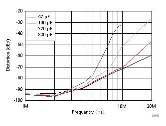
±VCC = ±7.5 V, RF = 158 Ω, AV = 5 V/V, VOUT = 10 VPP, see Figure 6-43 for RS value
Figure 6-46 HD3 vs Load Capacitance
GUID-18605300-9E4B-4EE9-8931-AEF71789747D-low.gif
±VCC = ±7.5 V, CLOAD = 150 pF, RF = 158 Ω, AV = 5 V/V, see Figure 6-43 for RS value.
Figure 6-48 Pulse Response