SBOS780C March 2016 – June 2021 THS3215
PRODUCTION DATA
- 1 Features
- 2 Applications
- 3 Description
- 4 Revision History
- 5 Pin Configuration and Functions
-
6 Specifications
- 6.1 Absolute Maximum Ratings
- 6.2 ESD Ratings
- 6.3 Recommended Operating Conditions
- 6.4 Thermal Information
- 6.5 Electrical Characteristics: D2S
- 6.6 Electrical Characteristics: OPS
- 6.7 Electrical Characteristics: D2S + OPS
- 6.8 Electrical Characteristics: Midscale (DC) Reference Buffer
- 6.9 Typical Characteristics: D2S + OPS
- 6.10 Typical Characteristics: D2S Only
- 6.11 Typical Characteristics: OPS Only
- 6.12 Typical Characteristics: Midscale (DC) Reference Buffer
- 6.13 Typical Characteristics: Switching Performance
- 6.14 Typical Characteristics: Gain Drift
- 7 Parameter Measurement Information
-
8 Detailed Description
- 8.1 Overview
- 8.2 Functional Block Diagram
- 8.3 Feature Description
- 8.4 Device Functional Modes
-
9 Application and Implementation
- 9.1
Application Information
- 9.1.1
Typical Applications
- 9.1.1.1 High-Frequency, High-Voltage, Dual-Output Line Driver for AWGs
- 9.1.1.2 High-Voltage Pulse-Generator
- 9.1.1.3 Single-Supply, AC-Coupled, Piezo Element Driver
- 9.1.1.4 Output Common-Mode Control Using the Midscale Buffer as a Level Shifter
- 9.1.1.5 Differential I/O Driver With independent Common-Mode Control
- 9.1.1
Typical Applications
- 9.1
Application Information
- 10Power Supply Recommendations
- 11Layout
- 12Device and Documentation Support
- 13Mechanical, Packaging, and Orderable Information
Package Options
Mechanical Data (Package|Pins)
- RGV|16
Thermal pad, mechanical data (Package|Pins)
- RGV|16
Orderable Information
7.1 Overview
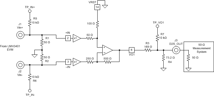
The THS3215 comprises three blocks of high-performance amplifiers. Each block requires both frequency-response and step-response characterization. The midscale buffer and OPS use standard, single-ended I/O test methods with network analyzers, pulse generators, and high-speed oscilloscopes. The differential to single-ended input stage (D2S) requires a wideband differential source for test purposes. All ac characterization tests were performed using the THS3215 evaluation module (EVM). The THS3215EVM offers many configuration options. For most of the D2S-only tests, the OPS was disabled. Figure 7-1 shows a typical configuration for an ac frequency-response test of the D2S.
The THS3215EVM includes unpopulated, optional, passive elements at the D2S inputs to implement a differential filter. These elements were not used in the D2S characterization, and the two input pins were terminated to ground through 49.9 Ω resistors. DC test points are provided through 10 kΩ or 20 kΩ resistors on all THS3215 nodes. Figure 7-1 also shows the output network used to emulate a 200 Ω load resistance (RLOAD) while presenting a 50 Ω source back to the D2S output pin. The R3 (= 169 Ω) and R4 (= 73.2 Ω) resistors combine with the 50 Ω network analyzer input impedance to present a 200 Ω load at VO1 (pin 6), The impedance presented from the input of the network analyzer back to the D2S output (VO1, pin 6) is 50 Ω. The 16.5 dB insertion loss intrinsic to this dc-coupled impedance network is removed from the characterization curves. VREF (pin 14) was connected to GND for all the tests.
 Figure 7-1 D2S Input and Output
Interface Showing 50 Ω Differential Input, and 200 Ω RLOAD at
VO1