SLOS224K July   1999  – May 2024 THS4031 , THS4032

PRODUCTION DATA  

  1.   1
  2. Features
  3. Applications
  4. Description
  5. Pin Configuration and Functions
  6. Specifications
    1. 5.1  Absolute Maximum Ratings
    2. 5.2  ESD Ratings
    3. 5.3  Recommended Operating Conditions
    4. 5.4  Thermal Information - THS4031
    5. 5.5  Thermal Information - THS4032
    6. 5.6  Electrical Characteristics - THS4031, RL = 150Ω
    7. 5.7  Electrical Characteristics - THS4031, RL = 1kΩ
    8. 5.8  Electrical Characteristics - THS4032, RL = 150Ω
    9. 5.9  Electrical Characteristics - THS4032, RL = 1kΩ
    10. 5.10 Typical Characteristics - THS4031
    11. 5.11 Typical Characteristics - THS4032
  7. Detailed Description
    1. 6.1 Overview
    2. 6.2 Functional Block Diagrams
    3. 6.3 Feature Description
      1. 6.3.1 Offset Nulling
    4. 6.4 Device Functional Modes
  8. Application and Implementation
    1. 7.1 Application Information
      1. 7.1.1 Driving a Capacitive Load
      2. 7.1.2 Low-Pass Filter Configurations
    2. 7.2 Typical Application
      1. 7.2.1 Design Requirements
      2. 7.2.2 Detailed Design Procedure
        1. 7.2.2.1 Selection of Multiplexer
        2. 7.2.2.2 Signal Source
        3. 7.2.2.3 Driving Amplifier
        4. 7.2.2.4 Driving Amplifier Bandwidth Restriction
      3. 7.2.3 Application Curves
    3. 7.3 Power Supply Recommendations
    4. 7.4 Layout
      1. 7.4.1 Layout Guidelines
        1. 7.4.1.1 General PowerPAD™ Integrated Circuit Package Design Considerations
      2. 7.4.2 Layout Example
  9. Device and Documentation Support
    1. 8.1 Documentation Support
      1. 8.1.1 Related Documentation
    2. 8.2 Receiving Notification of Documentation Updates
    3. 8.3 Support Resources
    4. 8.4 Trademarks
    5. 8.5 Electrostatic Discharge Caution
    6. 8.6 Glossary
  10. Revision History
  11. 10Mechanical, Packaging, and Orderable Information

Package Options

Refer to the PDF data sheet for device specific package drawings

Mechanical Data (Package|Pins)
  • D|8
  • DGN|8
Thermal pad, mechanical data (Package|Pins)
Orderable Information

Offset Nulling

The THS403x have a very low input offset voltage for high-speed amplifiers. However, if additional correction is required, an offset nulling function has been provided on the THS4031. To adjust the input offset voltage, place a potentiometer between pin 1 and pin 8 of the device, and tie the wiper to the negative supply. Figure 6-4 shows this feature.
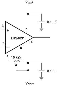
THS4031 THS4032 Offset
                    Nulling Schematic Figure 6-4 Offset Nulling Schematic