SLOS547A November 2008 – November 2015 THS4509-Q1
PRODUCTION DATA.
- 1 Features
- 2 Applications
- 3 Description
- 4 Revision History
- 5 Pin Configuration and Functions
- 6 Specifications
- 7 Detailed Description
-
8 Application and Implementation
- 8.1 Application Information
- 8.2 Typical Applications
- 9 Power Supply Recommendations
- 10Layout
- 11Device and Documentation Support
- 12Mechanical, Packaging, and Orderable Information
Package Options
Mechanical Data (Package|Pins)
- RGT|16
Thermal pad, mechanical data (Package|Pins)
- RGT|16
Orderable Information
10 Layout
10.1 Layout Guidelines
TI recommends following the layout of the external components near the amplifier, ground plane construction, and power routing of the EVM as closely as possible. General guidelines are:
- Signal routing should be direct and as short as possible into and out of the op amp circuit.
- The feedback path should be short and direct avoiding vias.
- Ground or power planes should be removed from directly under the amplifier’s input and output pins.
- An output resistor is recommended on each output, as near to the output pin as possible.
- Two 10-μF and two 0.1-μF power-supply decoupling capacitors should be placed as near to the power-supply pins as possible.
- Two 0.1-μF capacitors should be placed between the CM input pins and ground. This limits noise coupled into the pins. One each should be placed to ground near pin 4 and pin 9.
- It is recommended to split the ground pane on layer 2 (L2) and to use a solid ground on layer 3 (L3). A single-point connection should be used between each split section on L2 and L3.
- A single-point connection to ground on L2 is recommended for the input termination resistors R1 and R2. This should be applied to the input gain resistors if termination is not used.
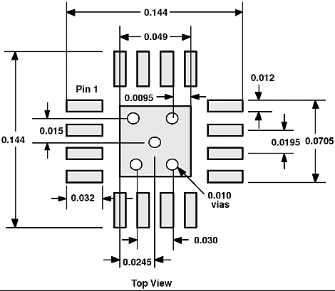
- The THS4509-Q1 recommended PCB footprint is shown in Figure 94.
 Figure 94. QFN Etch and Via Pattern
10.1.1 THS4509-Q1 EVM
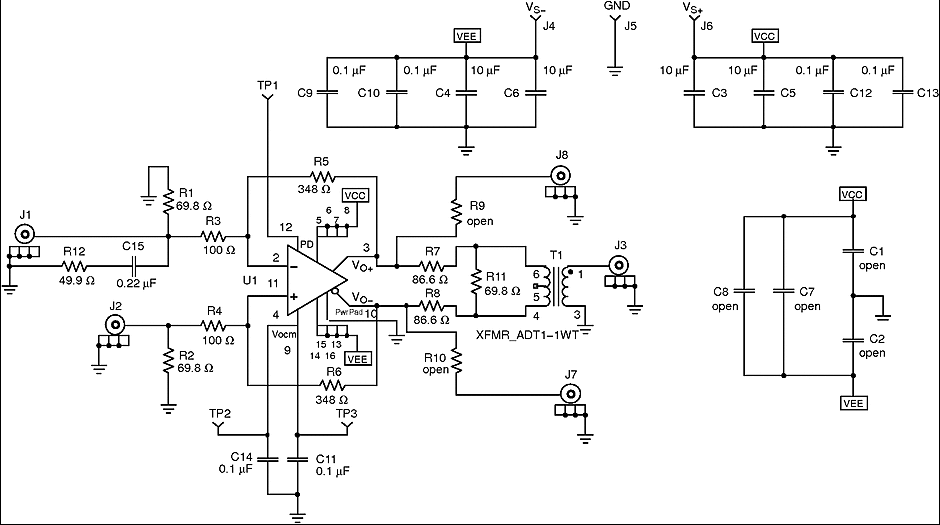
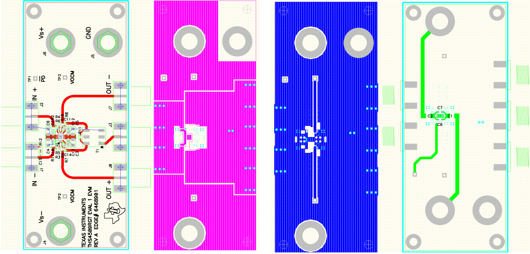
Figure 95 is the THS4509-Q1 EVAL1 EVM schematic, layers 1 through 4 of the PCB are shown in Figure 96, and Table 6 is the bill of material for the EVM as supplied from TI.
 Figure 95. THS4509-Q1 EVAL1 EVM Schematic
Table 6. THS4509-Q1 EVAL1 EVM Bill Of Materials
| ITEM | DESCRIPTION | SMD SIZE |
REFERENCE DESIGNATOR |
PCB QTY |
MANUFACTURER'S PART NUMBER |
|---|---|---|---|---|---|
| 1 | CAPACITOR, 10 µF, ceramic, X5R, 6.3 V | 0805 | C3, C4, C5, C6 | 4 | (AVX) 08056D106KAT2A |
| 2 | CAPACITOR, 0.1 µF, ceramic, X5R, 10 V | 0402 | C9, C10, C11, C12, C13, C14 | 6 | (AVX) 0402ZD104KAT2A |
| 3 | CAPACITOR, 0.22 µF, ceramic, X5R, 6.3 V | 0402 | C15 | 1 | (AVX) 04026D224KAT2A |
| 4 | OPEN | 0402 | C1, C2, C7, C8 | 4 | |
| 5 | OPEN | 0402 | R9, R10 | 2 | |
| 6 | Resistor, 49.9 Ω, 1/16 W, 1% | 0402 | R12 | 1 | (KOA) RK73H1ETTP49R9F |
| 8 | Resistor, 69.8 Ω, 1/16 W, 1% | 0402 | R1, R2, R11 | 3 | (KOA) RK73H1ETTP69R8F |
| 9 | Resistor, 86.6 Ω, 1/16 W, 1% | 0402 | R7, R8 | 2 | (KOA) RK73H1ETTP86R6F |
| 10 | Resistor, 100 Ω, 1/16 W, 1% | 0402 | R3, R4 | 2 | (KOA) RK73H1ETTP1000F |
| 11 | Resistor, 348 Ω, 1/16 W, 1% | 0402 | R5, R6 | 2 | (KOA) RK73H1ETTP3480F |
| 12 | Transformer, RF | T1 | 1 | (MINI-CIRCUITS) ADT1-1WT | |
| 13 | Jack, banana receptacle, 0.25" diameter hole |
J4, J5, J6 | 3 | (HH SMITH) 101 | |
| 14 | OPEN | J1, J7, J8 | 3 | ||
| 15 | Connector, edge, SMA PCB jack | J2, J3 | 2 | (JOHNSON) 142-0701-801 | |
| 16 | Test point, red | TP1, TP2, TP3 | 3 | (KEYSTONE) 5000 | |
| 17 | IC, THS4509 | U1 | 1 | (TI) THS4509RGT | |
| 18 | Standoff, 4-40 HEX, 0.625" length | 4 | (KEYSTONE) 1808 | ||
| 19 | Screw, phillips, 4-40, 0.250" | 4 | SHR-0440-016-SN | ||
| 20 | Printed-circuit-board | 1 | (TI) EDGE# 6468901 |
10.1.2 EVM Warnings and Restrictions
It is important to operate this EVM within the input and output voltage ranges below:
- Input Range, VI: 3 V to 6 V not to exceed VS+ or VS-
- Output range, VO: 3 V to 6 V not to exceed VS+ or VS-
Exceeding the specified input range may cause unexpected operation and/or irreversible damage to the EVM. If there are questions concerning the input range, please contact a TI field representative prior to connecting the input power.
Applying loads outside of the specified output range may result in unintended operation and/or possible permanent damage to the EVM. Please consult the product data sheet or EVM user's guide (if user's guide is available) prior to connecting any load to the EVM output. If there is uncertainty as to the load specification, please contact a TI field representative.
During normal operation, some circuit components may have case temperatures greater than 30°C. The EVM is designed to operate properly with certain components above 50°C as long as the input and output ranges are maintained. These components include but are not limited to linear regulators, switching transistors, pass transistors, and current sense resistors. These types of devices can be identified using the EVM schematic located in the material provided. When placing measurement probes near these devices during operation, please be aware that these devices may be very warm to the touch.
10.2 Layout Example
 Figure 96. THS4509-Q1 EVAL1 EVM Layer 1 Through 4