SLOS547A November 2008 – November 2015 THS4509-Q1
PRODUCTION DATA.
- 1 Features
- 2 Applications
- 3 Description
- 4 Revision History
- 5 Pin Configuration and Functions
- 6 Specifications
- 7 Detailed Description
-
8 Application and Implementation
- 8.1 Application Information
- 8.2 Typical Applications
- 9 Power Supply Recommendations
- 10Layout
- 11Device and Documentation Support
- 12Mechanical, Packaging, and Orderable Information
Package Options
Mechanical Data (Package|Pins)
- RGT|16
Thermal pad, mechanical data (Package|Pins)
- RGT|16
Orderable Information
6 Specifications
6.1 Absolute Maximum Ratings
over operating free-air temperature range (unless otherwise noted)(1)| MIN | MAX | UNIT | |||
|---|---|---|---|---|---|
| VS– to VS+ | Supply voltage | 6 | V | ||
| VI | Input voltage | –VS | +VS | ||
| VID | Differential input voltage | 4 | V | ||
| IO | Output current(2) | 200 | mA | ||
| Continuous power dissipation | See Thermal Information | ||||
| TJ | Maximum junction temperature | 150 | °C | ||
| TA | Operating free-air temperature | –40 | 125 | °C | |
| Tstg | Storage temperature | –65 | 150 | °C | |
(1) Stresses beyond those listed under Absolute Maximum Ratings may cause permanent damage to the device. These are stress ratings only, which do not imply functional operation of the device at these or any other conditions beyond those indicated under Recommended Operating Conditions. Exposure to absolute-maximum-rated conditions for extended periods may affect device reliability.
(2) The THS4509-Q1 incorporates a (QFN) exposed thermal pad on the underside of the chip. This acts as a heatsink and must be connected to a thermally dissipative plane for proper power dissipation. Failure to do so may result in exceeding the maximum junction temperature, which could permanently damage the device. See TI technical brief SLMA002 and SLMA004 for more information about utilizing the QFN thermally enhanced package.
6.2 ESD Ratings
| VALUE | UNIT | |||
|---|---|---|---|---|
| V(ESD) | Electrostatic discharge | Human-body model (HBM), per AEC Q100-002(1) | ±2000 | V |
| Charged-device model (CDM), per AEC Q100-011 | ±1500 | |||
| Machine Model (MM) | ±100 | |||
(1) AEC Q100-002 indicates that HBM stressing shall be in accordance with the ANSI/ESDA/JEDEC JS-001 specification.
6.3 Recommended Operating Conditions
over operating free-air temperature range (unless otherwise noted)| MIN | NOM | MAX | UNIT | ||
|---|---|---|---|---|---|
| Total supply voltage | 3 | 5 | V | ||
| Operating temperature, TJ | –40 | 25 | 125 | °C | |
6.4 Thermal Information
| THERMAL METRIC(1) | THS4509-Q1 | UNIT | |
|---|---|---|---|
| RGT (QFN) | |||
| 16-PIN | |||
| RθJA | Junction-to-ambient thermal resistance | 50.8 | °C/W |
| RθJC(top) | Junction-to-case (top) thermal resistance | 67.7 | °C/W |
| RθJB | Junction-to-board thermal resistance | 24.5 | °C/W |
| ψJT | Junction-to-top characterization parameter | 2 | °C/W |
| ψJB | Junction-to-board characterization parameter | 24.5 | °C/W |
| RθJC(bot) | Junction-to-case (bottom) thermal resistance | 8.2 | °C/W |
(1) For more information about traditional and new thermal metrics, see the Semiconductor and IC Package Thermal Metrics application report, SPRA953.
6.5 Electrical Characteristics: VS+ – VS– = 5 V
test conditions (unless otherwise noted): VS+ = 2.5 V, VS– = –2.5 V, G = 10 dB, CM = open, VO = 2 Vpp, RF = 349 Ω, RL = 200 Ω differential, TA = 25°C, single-ended input, differential output, input and output referenced to mid-supply| PARAMETER | TEST CONDITIONS | TEST LEVEL(1) | MIN | TYP | MAX | UNIT | ||
|---|---|---|---|---|---|---|---|---|
| AC PERFORMANCE | ||||||||
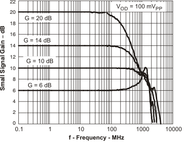
| Small-signal bandwidth | G = 6 dB, VO = 100 mVpp | C | 2 | GHz | ||||
| G = 10 dB, VO = 100 mVpp | 1.9 | |||||||
| G = 14 dB, VO = 100 mVpp | 600 | MHz | ||||||
| G = 20 dB, VO = 100 mVpp | 275 | |||||||
| Gain-bandwidth product | G = 20 dB | 3 | GHz | |||||
| Bandwidth for 0.1-dB flatness | G = 10 dB, VO = 2 Vpp | 300 | MHz | |||||
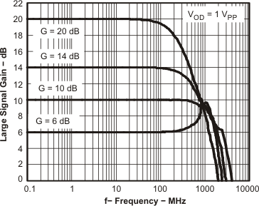
| Large-signal bandwidth | G = 10 dB, VO = 2 Vpp | 1.5 | GHz | |||||
| Slew rate (differential) | 2-V step | 6600 | V/μs | |||||
| Rise time | 2-V step | 0.5 | ns | |||||
| Fall time | 2-V step | 0.5 | ns | |||||
| Settling time to 1% | 2-V step | 2 | ns | |||||
| Settling time to 0.1% | 2-V step | 10 | ns | |||||
| Second-order harmonic distortion | f = 10 MHz | –104 | dBc | |||||
| f = 50 MHz | –80 | |||||||
| f = 100 MHz | –68 | |||||||
| Third-order harmonic distortion | f = 10 MHz | –108 | dBc | |||||
| f = 50 MHz | –92 | |||||||
| f = 100 MHz | –81 | |||||||
| Second-order intermodulation distortion | 200-kHz tone spacing, RL = 499 Ω |
fC = 70 MHz | –78 | dBc | ||||
| fC = 140 MHz | –64 | |||||||
| Third-order intermodulation distortion | 200-kHz tone spacing, RL = 499 Ω |
fC = 70 MHz | –95 | dBc | ||||
| fC = 140 MHz | –78 | |||||||
| Second-order output intercept point | 200-kHz tone spacing, RL = 100 Ω, referenced to 50-Ω output |
fC = 70 MHz | 78 | dBm | ||||
| fC = 140 MHz | 58 | |||||||
| Third-order output intercept point | 200-kHz tone spacing, RL = 100 Ω, referenced to 50-Ω output |
fC = 70 MHz | 43 | dBm | ||||
| fC = 140 MHz | 38 | |||||||
| 1-dB compression point | fC = 70 MHz | 12.2 | dBm | |||||
| fC = 140 MHz | 10.8 | |||||||
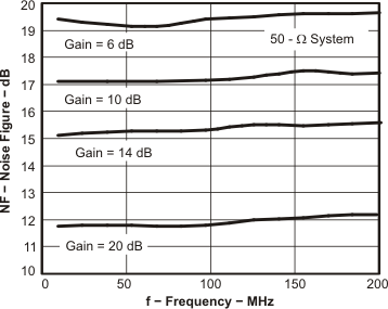
| Noise figure | 50-Ω system, 10 MHz | 17.1 | dB | |||||
| Input voltage noise | f > 10 MHz | 1.9 | nV/√Hz | |||||
| Input current noise | f > 10 MHz | 2.2 | pA/√Hz | |||||
| DC PERFORMANCE | ||||||||
| Open-loop voltage gain (AOL) | C | 68 | dB | |||||
| Input offset voltage | TA = 25°C | A | 1 | 4 | mV | |||
| TA = –40°C to 125°C | 1 | 5 | mV | |||||
| Average input offset voltage drift | TA = –40°C to 125°C | B | 2.6 | µV/°C | ||||
| Input bias current | TA = 25°C | A | 8 | 15.5 | µA | |||
| TA = –40°C to 125°C | 8 | 18.5 | ||||||
| Average input bias current drift | TA = –40°C to 125°C | B | 20 | nA/°C | ||||
| Input offset current | TA = 25°C | A | 1.6 | 3.6 | µA | |||
| TA = –40°C to 125°C | 1.6 | 7 | ||||||
| Average input offset current drift | TA = –40°C to 125°C | B | 4 | nA/°C | ||||
| INPUT | ||||||||
| Common-mode input range high | B | 1.75 | V | |||||
| Common-mode input range low | –1.75 | |||||||
| Common-mode rejection ratio | 90 | dB | ||||||
| Differential input impedance | C | 1.35 || 1.77 | MΩ || pF | |||||
| Common-mode input impedance | C | 1.02 || 2.26 | MΩ || pF | |||||
| OUTPUT | ||||||||
| Maximum output voltage high | Each output with 100 Ω to mid-supply | TA = 25°C | A | 1.2 | 1.4 | V | ||
| TA = –40°C to 125°C | 1.1 | 1.4 | ||||||
| Minimum output voltage low | Each output with 100 Ω to mid-supply | TA = 25°C | –1.4 | –1.2 | V | |||
| TA = –40°C to 125°C | –1.4 | –1.1 | ||||||
| Differential output voltage swing | C | 4.8 | 5.6 | V | ||||
| TA = –40°C to 125°C | 4.4 | |||||||
| Differential output current drive | RL = 10 Ω | 96 | mA | |||||
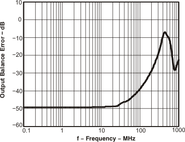
| Output balance error | VO = 100 mV, f = 1 MHz | –49 | dB | |||||
| Closed-loop output impedance | f = 1 MHz | 0.3 | Ω | |||||
| OUTPUT COMMON-MODE VOLTAGE CONTROL | ||||||||
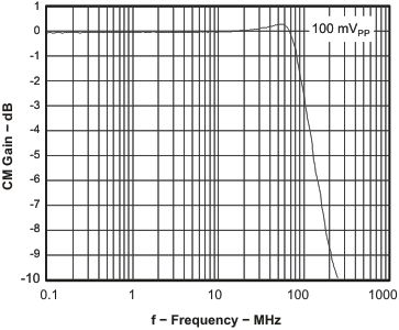
| Small-signal bandwidth | C | 700 | MHz | |||||
| Slew rate | 110 | V/μs | ||||||
| Gain | 1 | V/V | ||||||
| Output common-mode offset from CM input |
1.25 V < CM < 3.5 V | 5 | mV | |||||
| CM input bias current | 1.25 V < CM < 3.5 V | ±40 | µA | |||||
| CM input voltage range | –1.5 to 1.5 | V | ||||||
| CM input impedance | 23 || 1 | kΩ || pF | ||||||
| CM default voltage | 0 | V | ||||||
| POWER SUPPLY | ||||||||
| Specified operating voltage | C | 3 | 5 | 5.25 | V | |||
| Maximum quiescent current | TA = 25°C | A | 37.7 | 40.9 | mA | |||
| TA = –40°C to 125°C | 37.7 | 41.9 | ||||||
| Minimum quiescent current | TA = 25°C | 34.5 | 37.7 | mA | ||||
| TA = –40°C to 125°C | 33.5 | 37.7 | ||||||
| Power-supply rejection (±PSRR) | C | 90 | dB | |||||
| POWER DOWN | Referenced to Vs– | |||||||
| Enable voltage threshold | Assured on above 2.1 V + VS– | C | >2.1 + VS– | V | ||||
| Disable voltage threshold | Assured off below 0.7 V + VS– | <0.7 + VS– | V | |||||
| Powerdown quiescent current | TA = 25°C | A | 0.65 | 0.9 | mA | |||
| TA = –40°C to 125°C | 0.65 | 1 | ||||||
| Input bias current | PD = VS– | C | 100 | µA | ||||
| Input impedance | 50 || 2 | kΩ || pF | ||||||
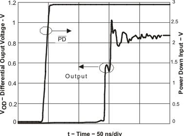
| Turn-on time delay | Measured to output on | 55 | ns | |||||
| Turn-off time delay | Measured to output off | 10 | µs | |||||
(1) Test levels: A = 100% tested at 25°C, overtemperature limits by characterization and simulation; B = Limits set by characterization and simulation; C = Typical value only for information.
6.6 Electrical Characteristics: VS+ – VS– = 3 V
test conditions (unless otherwise noted): VS+ = 1.5 V, VS– = –1.5 V, G = 10 dB, CM = open, VO = 1 Vpp, RF = 349 Ω, RL = 200 Ω differential, TA = 25°C, single-ended input, differential output, input and output referenced to mid-supply| PARAMETER | TEST CONDITIONS | TEST LEVEL(1) | MIN | TYP | MAX | UNIT | ||
|---|---|---|---|---|---|---|---|---|
| AC PERFORMANCE | ||||||||
| Small-signal bandwidth | G = 6 dB, VO = 100 mVpp | C | 1.9 | GHz | ||||
| G = 10 dB, VO = 100 mVpp | 1.6 | |||||||
| G = 14 dB, VO = 100 mVpp | 625 | MHz | ||||||
| G = 20 dB, VO = 100 mVpp | 260 | |||||||
| Gain-bandwidth product | G = 20 dB | 3 | GHz | |||||
| Bandwidth for 0.1-dB flatness | G = 10 dB, VO = 1 Vpp | 400 | MHz | |||||
| Large-signal bandwidth | G = 10 dB, VO = 1 Vpp | 1.5 | GHz | |||||
| Slew rate (differential) | 2-V step | 3500 | V/μs | |||||
| Rise time | 2-V step | 0.25 | ns | |||||
| Fall time | 2-V step | 0.25 | ns | |||||
| Settling time to 1% | 2-V step | 1 | ns | |||||
| Settling time to 0.1% | 2-V step | 10 | ns | |||||
| Second-order harmonic distortion | f = 10 MHz | –107 | dBc | |||||
| f = 50 MHz | –83 | |||||||
| f = 100 MHz | –60 | |||||||
| Third-order harmonic distortion | f = 10 MHz | –87 | dBc | |||||
| f = 50 MHz | –65 | |||||||
| f = 100 MHz | –54 | |||||||
| Second-order intermodulation distortion | 200-kHz tone spacing, RL = 499 Ω |
fC = 70 MHz | –77 | dBc | ||||
| fC = 140 MHz | –54 | |||||||
| Third-order intermodulation distortion | 200-kHz tone spacing, RL = 499 Ω |
fC = 70 MHz | –77 | dBc | ||||
| fC = 140 MHz | –62 | |||||||
| Second-order output intercept point | 200-kHz tone spacing RL = 100 Ω |
fC = 70 MHz | 72 | dBm | ||||
| fC = 140 MHz | 52 | |||||||
| Third-order output intercept point | 200-kHz tone spacing RL = 100 Ω |
fC = 70 MHz | 38.5 | dBm | ||||
| fC = 140 MHz | 30 | |||||||
| 1-dB compression point | fC = 70 MHz | 2.2 | dBm | |||||
| fC = 140 MHz | 0.25 | |||||||
| Noise figure | 50-Ω system, 10 MHz | 17.1 | dB | |||||
| Input voltage noise | f > 10 MHz | 1.9 | nV/√Hz | |||||
| Input current noise | f > 10 MHz | 2.2 | pA/√Hz | |||||
| DC PERFORMANCE | ||||||||
| Open-loop voltage gain (AOL) | C | 68 | dB | |||||
| Input offset voltage | TA = 25°C | 1 | mV | |||||
| Average input offset voltage drift | TA = –40°C to 125°C | 2.6 | µV/°C | |||||
| Input bias current | TA = 25°C | 6 | µA | |||||
| Average input bias current drift | TA = –40°C to 125°C | 20 | nA/°C | |||||
| Input offset current | TA = 25°C | 1.6 | µA | |||||
| Average input offset current drift | TA = –40°C to 125°C | 4 | nA/°C | |||||
| INPUT | ||||||||
| Common-mode input range high | B | 0.75 | V | |||||
| Common-mode input range low | –0.75 | V | ||||||
| Common-mode rejection ratio | 80 | dB | ||||||
| Differential input impedance | C | 1.35 || 1.77 | MΩ || pF | |||||
| Common-mode input impedance | C | 1.02 || 2.26 | MΩ || pF | |||||
| OUTPUT | ||||||||
| Maximum output voltage high | Each output with 100 Ω to mid-supply | TA = 25°C | C | 0.45 | V | |||
| Minimum output voltage low | Each output with 100 Ω to mid-supply | TA = 25°C | –0.45 | V | ||||
| Differential output voltage swing | 1.8 | V | ||||||
| Differential output current drive | RL = 10 Ω | 50 | mA | |||||
| Output balance error | VO = 100 mV, f = 1 MHz | –49 | dB | |||||
| Closed-loop output impedance | f = 1 MHz | 0.3 | Ω | |||||
| OUTPUT COMMON-MODE VOLTAGE CONTROL | ||||||||
| Small-signal bandwidth | C | 570 | MHz | |||||
| Slew rate | 60 | V/μs | ||||||
| Gain | 1 | V/V | ||||||
| Output common-mode offset from CM input |
1.25 V < CM < 3.5 V | 4 | mV | |||||
| CM input bias current | 1.25 V < CM < 3.5 V | ±40 | µA | |||||
| CM input voltage range | –1.5 to 1.5 | V | ||||||
| CM input impedance | 20 || 1 | kΩ || pF | ||||||
| CM default voltage | 0 | V | ||||||
| POWER SUPPLY | ||||||||
| Specified operating voltage | C | 3 | V | |||||
| Quiescent current | TA = 25°C | A | 34.8 | mA | ||||
| Power-supply rejection (±PSRR) | C | 70 | dB | |||||
| POWER DOWN | Referenced to Vs– | |||||||
| Enable voltage threshold | Assured on above 2.1 V + VS– | C | >2.1 + VS– | V | ||||
| Disable voltage threshold | Assured off below 0.7 V + VS– | <0.7 + VS– | V | |||||
| Power-down quiescent current | 0.46 | mA | ||||||
| Input bias current | PD = VS– | 65 | µA | |||||
| Input impedance | 50 || 2 | kΩ || pF | ||||||
| Turn-on time delay | Measured to output on | 100 | ns | |||||
| Turn-off time delay | Measured to output off | 10 | µs | |||||
(1) Test levels: A = 100% tested at 25°C, overtemperature limits by characterization and simulation; B = Limits set by characterization and simulation; C = Typical value only for information.
6.7 Typical Characteristics
6.7.1 Typical Characteristics: VS+ – VS– = 5 V
test conditions (unless otherwise noted): VS+ = 2.5 V, VS– = –2.5 V, CM = open, VO = 2 Vpp, RF = 349 Ω, RL = 200 Ω differential, G = 10 dB, single-ended input, input and output referenced to midrailTable 1. Table of Graphs VS+ – VS– = 5 V
| TYPICAL CHARACTERISTIC CURVE | FIGURE NO. | ||
|---|---|---|---|
| Small-signal frequency response | Figure 1 | ||
| Large-signal frequency response | Figure 2 | ||
| Harmonic distortion | HD2, G = 6 dB, VOD = 2 VPP | vs Frequency | Figure 3 |
| HD3, G = 6 dB, VOD = 2 VPP | vs Frequency | Figure 4 | |
| HD2, G = 10 dB, VOD = 2 VPP | vs Frequency | Figure 5 | |
| HD3, G = 10 dB, VOD = 2 VPP | vs Frequency | Figure 6 | |
| HD2, G = 14 dB, VOD = 2 VPP | vs Frequency | Figure 7 | |
| HD3, G = 14 dB, VOD = 2 VPP | vs Frequency | Figure 8 | |
| HD2, G = 10 dB | vs Output voltage | Figure 9 | |
| HD3, G = 10 dB | vs Output voltage | Figure 10 | |
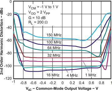
| HD2, G = 10 dB | vs Common-mode output voltage | Figure 11 | |
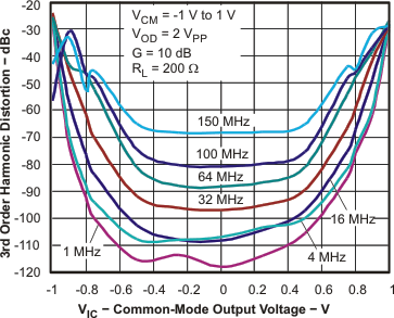
| HD3, G = 10 dB | vs Common-mode output voltage | Figure 12 | |
| Intermodulation distortion | IMD2, G = 6 dB, VOD = 2 VPP | vs Frequency | Figure 13 |
| IMD3, G = 6 dB, VOD = 2 VPP | vs Frequency | Figure 14 | |
| IMD2, G = 10 dB, VOD = 2 VPP | vs Frequency | Figure 15 | |
| IMD3, G = 10 dB, VOD = 2 VPP | vs Frequency | Figure 16 | |
| IMD2, G = 14 dB, VOD = 2 VPP | vs Frequency | Figure 17 | |
| IMD3, G = 14 dB, VOD = 2 VPP | vs Frequency | Figure 18 | |
| Output intercept point | OIP2 | vs Frequency | Figure 19 |
| OIP3 | vs Frequency | Figure 20 | |
| 0.1-dB flatness | Figure 21 | ||
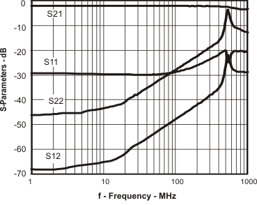
| S-parameters | vs Frequency | Figure 22 | |
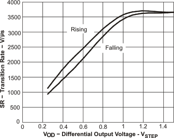
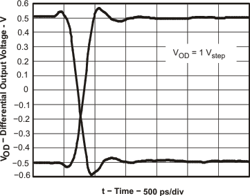
| Transition rate | vs Output voltage | Figure 23 | |
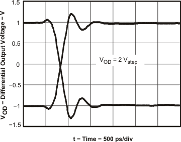
| Transient response | Figure 24 | ||
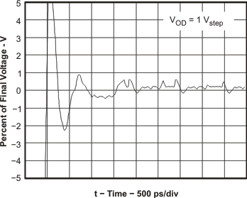
| Settling time | Figure 25 | ||
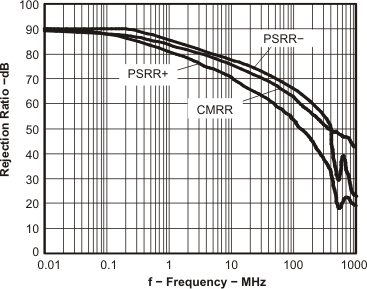
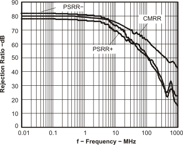
| Rejection ratio | vs Frequency | Figure 26 | |
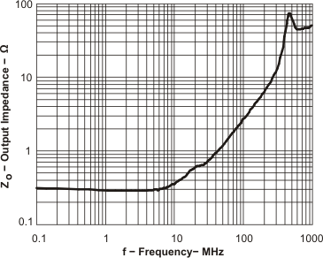
| Output impedance | vs Frequency | Figure 27 | |
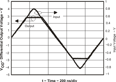
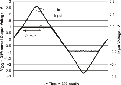
| Overdrive recovery | Figure 28 | ||
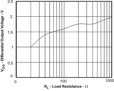
| Output voltage swing | vs Load resistance | Figure 29 | |
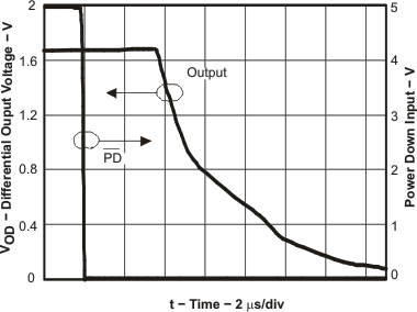
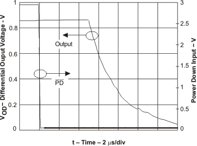
| Turn-off time | Figure 30 | ||
| Turn-on time | Figure 31 | ||
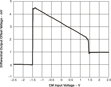
| Input offset voltage | vs Input common-mode voltage | Figure 32 | |
| Open-loop gain and phase | vs Frequency | Figure 33 | |
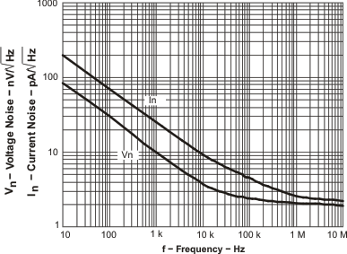
| Input referred noise | vs Frequency | Figure 34 | |
| Noise figure | vs Frequency | Figure 35 | |
| Quiescent current | vs Supply voltage | Figure 36 | |
| Power-supply current | vs Supply voltage in power-down mode | Figure 37 | |
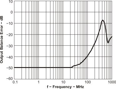
| Output balance error | vs Frequency | Figure 38 | |
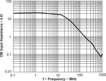
| CM input impedance | vs Frequency | Figure 39 | |
| CM small-signal frequency response | Figure 40 | ||
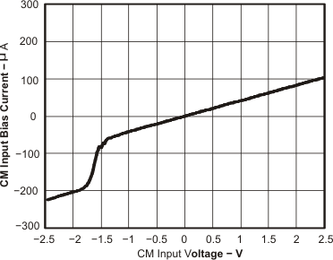
| CM input bias current | vs CM input voltage | Figure 41 | |
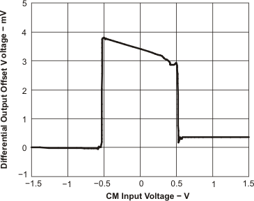
| Differential output offset voltage | vs CM input voltage | Figure 42 | |
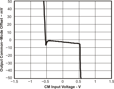
| Output common-mode offset | vs CM input voltage | Figure 43 | |
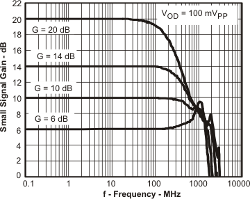
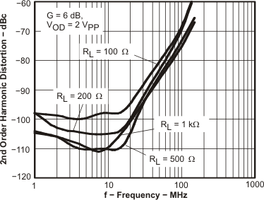
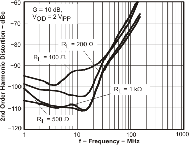
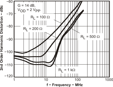
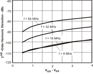
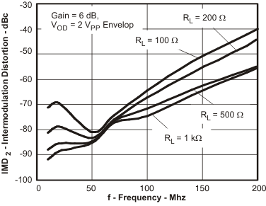
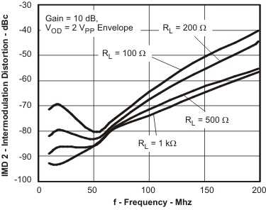
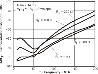
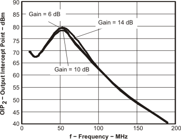
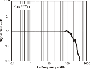
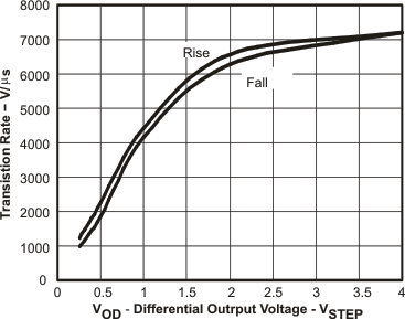
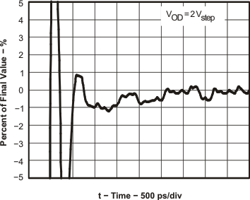
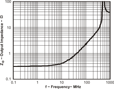
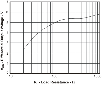
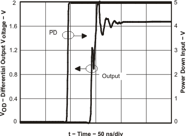
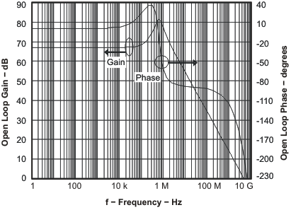
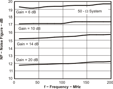
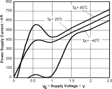
vs Supply Voltage in Power-Down Mode
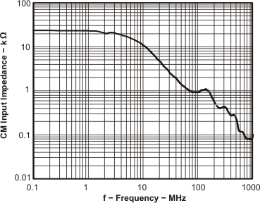
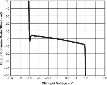
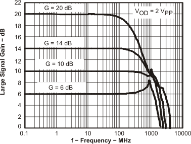
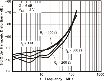
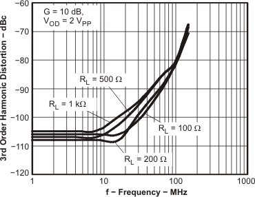
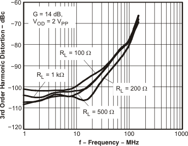
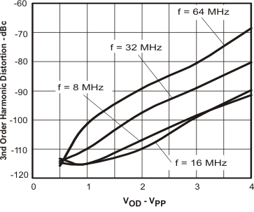
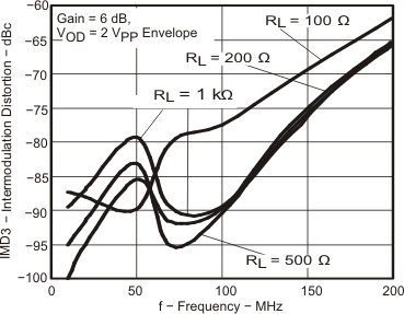
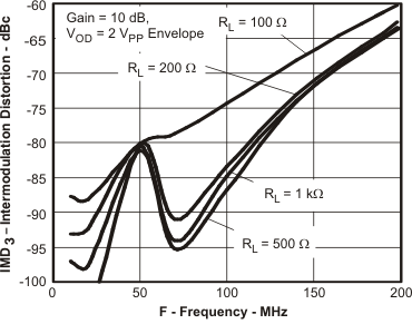
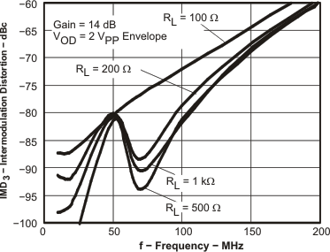
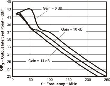
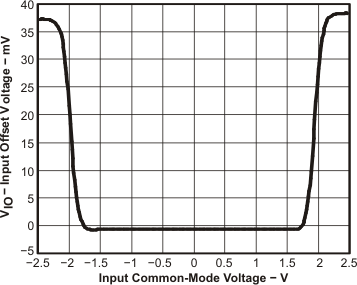
vs Input Common-Mode Voltage
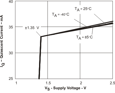
vs CM Input Voltage
6.7.2 Typical Characteristics: VS+ – VS– = 3 V
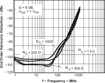
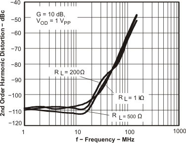
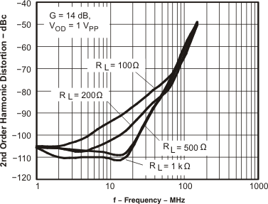
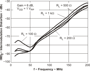
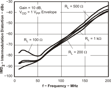
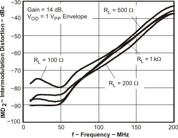
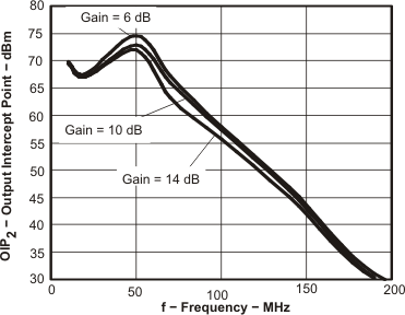
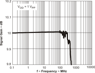
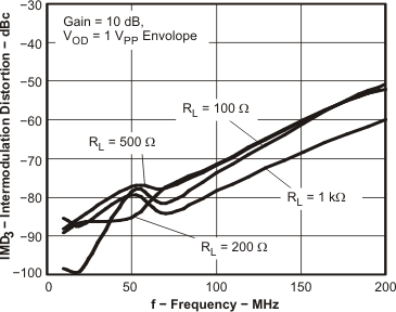
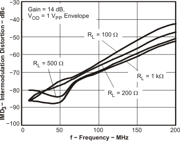
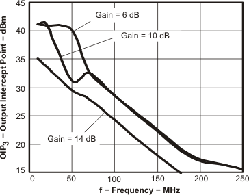
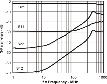
test conditions (unless otherwise noted): VS+ = 1.5 V, VS– = –1.5 V, CM = open, VOD = 1 Vpp, RF = 349 Ω,RL = 200 Ω differential, G = 10 dB, single-ended input, input and output referenced to midrail
Table 2. Table of Graphs VS+ – VS– = 3 V
| TYPICAL CHARACTERISTIC CURVE | FIGURE NO. | ||
|---|---|---|---|
| Small-signal frequency response | Figure 44 | ||
| Large-signal frequency response | Figure 45 | ||
| Harmonic distortion | HD2, G = 6 dB, VOD = 1 VPP | vs Frequency | Figure 46 |
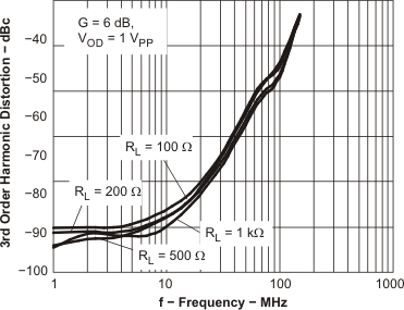
| HD3, G = 6 dB, VOD = 1 VPP | vs Frequency | Figure 47 | |
| HD2, G = 10 dB, VOD = 1 VPP | vs Frequency | Figure 48 | |
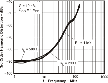
| HD3, G = 10 dB, VOD = 1 VPP | vs Frequency | Figure 49 | |
| HD2, G = 14 dB, VOD = 1 VPP | vs Frequency | Figure 50 | |
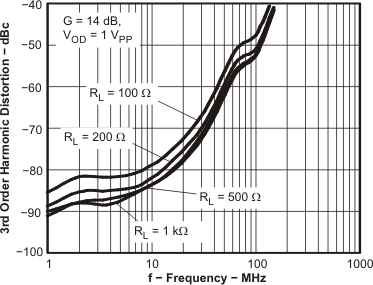
| HD3, G = 14 dB, VOD = 1 VPP | vs Frequency | Figure 51 | |
| Intermodulation distortion | IMD2, G = 6 dB, VOD = 1 VPP | vs Frequency | Figure 52 |
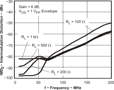
| IMD3, G = 6 dB, VOD = 1 VPP | vs Frequency | Figure 53 | |
| IMD2, G = 10 dB, VOD = 1 VPP | vs Frequency | Figure 54 | |
| IMD3, G = 10 dB, VOD = 1 VPP | vs Frequency | Figure 55 | |
| IMD2, G = 14 dB, VOD = 1 VPP | vs Frequency | Figure 56 | |
| IMD3, G = 14 dB, VOD = 1 VPP | vs Frequency | Figure 57 | |
| Output intercept point | OIP2 | vs Frequency | Figure 58 |
| OIP3 | vs Frequency | Figure 59 | |
| 0.1-dB flatness | Figure 60 | ||
| S-parameters | vs Frequency | Figure 61 | |
| Transition rate | vs Output voltage | Figure 62 | |
| Transient response | Figure 63 | ||
| Settling time | Figure 64 | ||
| Output voltage swing | vs Load resistance | Figure 65 | |
| Rejection ratio | vs Frequency | Figure 66 | |
| Overdrive recovery | Figure 67 | ||
| Output impedance | vs Frequency | Figure 68 | |
| Turn-off time | Figure 69 | ||
| Turn-on time | Figure 70 | ||
| Output balance error | vs Frequency | Figure 71 | |
| Noise figure | vs Frequency | Figure 72 | |
| CM input impedance | vs Frequency | Figure 73 | |
| Differential output offset voltage | vs CM input voltage | Figure 74 | |
| Output common-mode offset | vs CM input voltage | Figure 75 | |
vs CM Input Voltage
vs CM Input Voltage
